SLVSCC0D November 2013 – October 2019 DRV8850
PRODUCTION DATA.
- 1 Features
- 2 Applications
- 3 Description
- 4 Revision History
- 5 Pin Configuration and Functions
- 6 Specifications
-
7 Detailed Description
- 7.1 Overview
- 7.2 Functional Block Diagram
- 7.3 Feature Description
- 7.4 Device Functional Modes
- 8 Application and Implementation
- 9 Power Supply Recommendations
- 10Layout
- 11Device and Documentation Support
- 12Mechanical, Packaging, and Orderable Information
Package Options
Mechanical Data (Package|Pins)
- RGY|24
Thermal pad, mechanical data (Package|Pins)
- RGY|24
Orderable Information
7.3.3 Current Sensing – VPROPI
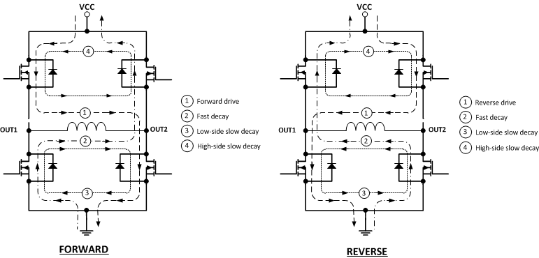
The VPROPI pin outputs an analog current that is proportional to the current flowing in the H-bridge. The output current is typically 1 / 2000 of the current in both high side FETs. VPROPI is derived from the current through either of the high side FETs. Because of this, VPROPI does not represent the H-bridge current when operating in a fast-decay mode or low-side slow-decay mode. VPROPI represents the H-bridge current under forward drive, reverse drive, and high-side slow decay. VPROPI output is delayed by roughly 2 µs after the high side FET is switched on and it has reached approximately VCC (including the deglitch on the HSon). Select the external resistor so that the voltage on VPROPI is less than (VCC – 1 V), so the resistor must be sized less than:

where IOUT is the maximum drive current to be monitored
The range of current that can be monitored is 500 mA to 5 A, assuming the external resistor meets Equation 1.
 Figure 14. Forward and Reverse Operation
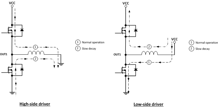
 When using an independent half-bridge as a high-side driver, VPROPI does not output a current measurement during slow decay. During typical operation, VPROPI represents the total current flowing to loads connected to OUT1 and OUT2.
VPROPI is nonfunctional when implemented as a low-side driver.
 Figure 15. High-Side and Low-Side Drivers