SLVSCC0D November 2013 – October 2019 DRV8850
PRODUCTION DATA.
- 1 Features
- 2 Applications
- 3 Description
- 4 Revision History
- 5 Pin Configuration and Functions
- 6 Specifications
-
7 Detailed Description
- 7.1 Overview
- 7.2 Functional Block Diagram
- 7.3 Feature Description
- 7.4 Device Functional Modes
- 8 Application and Implementation
- 9 Power Supply Recommendations
- 10Layout
- 11Device and Documentation Support
- 12Mechanical, Packaging, and Orderable Information
Package Options
Mechanical Data (Package|Pins)
- RGY|24
Thermal pad, mechanical data (Package|Pins)
- RGY|24
Orderable Information
7.3.8 LDO Voltage Regulator
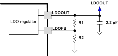
An LDO regulator is integrated into the DRV8850 device. The LDO regulator is typically used to provide the supply voltage for a low-power microcontroller. For proper operation, bypass the LDOOUT pin to GND using a ceramic capacitor. The recommended value for this component is 2.2 μF.
Two external resistors are used to set the LDO voltage (VLDO) by creating a voltage divider between LDOOUT and LDOFB. The LDO output voltage can be given by:

where
- R1 is located between LDOOUT and LDOFB
- R2 is between LDOFB and GND
 Figure 18. LDO Regulator Schematic
 The output voltage is adjustable from 1.6 V to VCC – VLDO using external resistors. The LDOEN pin is used to enable or disable the LDO regulator; when disabled, the output is turned off and the LDO regulator enters a very-low-power state.
When the LDO current load exceeds ICL, the LDO regulator behaves like a constant current source. The LDO output voltage drops significantly with currents greater than ICL.