SLVSDY7B October 2017 – January 2021 DRV8873-Q1
PRODUCTION DATA
- 1 Features
- 2 Applications
- 3 Description
- 4 Revision History
- 5 Pin Configuration and Functions
- 6 Specifications
-
7 Detailed Description
- 7.1 Overview
- 7.2 Functional Block Diagram
- 7.3 Feature Description
- 7.4 Device Functional Modes
- 7.5 Programming
- 7.6 Register Maps
- 8 Application and Implementation
- 9 Power Supply Recommendations
- 10Layout
- 11Device and Documentation Support
- 12Mechanical, Packaging, and Orderable Information
Package Options
Mechanical Data (Package|Pins)
- PWP|24
Thermal pad, mechanical data (Package|Pins)
- PWP|24
Orderable Information
7.3.1 Bridge Control
The device output has four N-channel MOSFETs configured in a H-bridge. The driver can be controlled using a PH/EN, PWM, or independent half-bridge input mode. Table 7-2 lists the control mode configurations.
| HARDWARE DEVICE MODE PIN | SPI DEVICE MODE REGISTER | CONTROL MODE |
|---|---|---|
| L | 00b | PH/EN |
| H | 01b (default) | PWM |
| 200 kΩ ± 5% to GND | 10b | Independent half bridge |
| Not applicable | 11b | Input disabled, bridge Hi-Z |
In the hardware version of the device, the MODE pin determines the control interface and latches on power-up or when exiting sleep mode. During the device power-up sequence, the DVDD pin is enabled first, and then the MODE pin latches. Tying the MODE pin directly to ground sets the mode to phase and enable. Tying the MODE pin to the DVDD pin, or an external 5 V rail, sets the mode to PWM. Connecting the MODE pin to ground with a 200 kΩ ± 5% resistor sets the mode to independent half-bridge where the two half-bridges can be independently controlled by their respective input (INx) pins. Table 7-3 lists the different MODE pin settings.
| CONNECTION | MODE | CIRCUIT |
|---|---|---|
| Connect to GND | Phase and Enable | 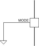 |
| 200 kΩ ± 5% to GND | Independent half-bridge | 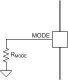 |
| Connect to DVDD | PWM | 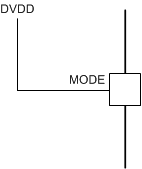 |
In the SPI version of the device, the mode setting can be changed by writing to the MODE register in the IC1 control register because this device version has no dedicated MODE pin. The device mode gets latched when the DISABLE signal transitions from high to low.