SLVSDS7B August   2019  – November 2019 DRV8876

PRODUCTION DATA.  

  1. Features
  2. Applications
  3. Description
    1.     Device Images
      1.      Simplified Schematic
  4. Revision History
  5. Pin Configuration and Functions
    1.     Pin Functions
  6. Specifications
    1. 6.1 Absolute Maximum Ratings
    2. 6.2 ESD Ratings
    3. 6.3 Recommended Operating Conditions
    4. 6.4 Thermal Information
    5. 6.5 Electrical Characteristics
    6. 6.6 Typical Characteristics
  7. Detailed Description
    1. 7.1 Overview
    2. 7.2 Functional Block Diagram
    3. 7.3 Feature Description
      1. 7.3.1 External Components
      2. 7.3.2 Control Modes
        1. 7.3.2.1 PH/EN Control Mode (PMODE = Logic Low)
        2. 7.3.2.2 PWM Control Mode (PMODE = Logic High)
        3. 7.3.2.3 Independent Half-Bridge Control Mode (PMODE = Hi-Z)
      3. 7.3.3 Current Sense and Regulation
        1. 7.3.3.1 Current Sensing
        2. 7.3.3.2 Current Regulation
          1. 7.3.3.2.1 Fixed Off-Time Current Chopping
          2. 7.3.3.2.2 Cycle-By-Cycle Current Chopping
      4. 7.3.4 Protection Circuits
        1. 7.3.4.1 VM Supply Undervoltage Lockout (UVLO)
        2. 7.3.4.2 VCP Charge Pump Undervoltage Lockout (CPUV)
        3. 7.3.4.3 OUTx Overcurrent Protection (OCP)
        4. 7.3.4.4 Thermal Shutdown (TSD)
        5. 7.3.4.5 Fault Condition Summary
      5. 7.3.5 Pin Diagrams
        1. 7.3.5.1 Logic-Level Inputs
        2. 7.3.5.2 Tri-Level Inputs
        3. 7.3.5.3 Quad-Level Inputs
    4. 7.4 Device Functional Modes
      1. 7.4.1 Active Mode
      2. 7.4.2 Low-Power Sleep Mode
      3. 7.4.3 Fault Mode
  8. Application and Implementation
    1. 8.1 Application Information
    2. 8.2 Typical Application
      1. 8.2.1 Primary Application
        1. 8.2.1.1 Design Requirements
        2. 8.2.1.2 Detailed Design Procedure
          1. 8.2.1.2.1 Current Sense and Regulation
          2. 8.2.1.2.2 Power Dissipation and Output Current Capability
          3. 8.2.1.2.3 Thermal Performance
            1. 8.2.1.2.3.1 Steady-State Thermal Performance
            2. 8.2.1.2.3.2 Transient Thermal Performance
        3. 8.2.1.3 Application Curves
      2. 8.2.2 Alternative Application
        1. 8.2.2.1 Design Requirements
        2. 8.2.2.2 Detailed Design Procedure
          1. 8.2.2.2.1 Current Sense and Regulation
        3. 8.2.2.3 Application Curves
  9. Power Supply Recommendations
    1. 9.1 Bulk Capacitance
  10. 10Layout
    1. 10.1 Layout Guidelines
    2. 10.2 Layout Example
      1. 10.2.1 HTSSOP Layout Example
      2. 10.2.2 VQFN Layout Example
  11. 11Device and Documentation Support
    1. 11.1 Documentation Support
      1. 11.1.1 Related Documentation
    2. 11.2 Receiving Notification of Documentation Updates
    3. 11.3 Community Resources
    4. 11.4 Trademarks
    5. 11.5 Electrostatic Discharge Caution
    6. 11.6 Glossary
  12. 12Mechanical, Packaging, and Orderable Information

Package Options

Refer to the PDF data sheet for device specific package drawings

Mechanical Data (Package|Pins)
  • RGT|16
  • PWP|16
Thermal pad, mechanical data (Package|Pins)
Orderable Information

Cycle-By-Cycle Current Chopping

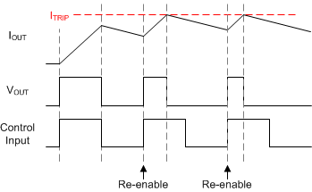
In cycle-by-cycle mode, the H-bridge enters a brake, low-side slow decay state (both low-side MOSFETs ON) after IOUT exceeds ITRIP until the next control input edge on the EN/IN1 or PH/IN2 pins. This allows for additional control of the current chopping scheme by the external controller. This is shown in Figure 13. Cycle-by-cycle mode will not support 100% duty cycle current regulation as a new control input edge is required to reset the outputs after the brake, low-side slow decay state has been entered.
DRV8876 drv887x-cbc.gifFigure 13. Cycle-By-Cycle Current Regulation

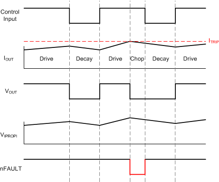
In cycle-by-cycle mode, the device will also indicates whenever the H-bridge has entered internal current chopping by pulling the nFAULT pin low. This can be used to determine when the device outputs will differ from the control inputs or the load has reached the ITRIP threshold. This is shown in Figure 14. nFAULT will be released whenever the next control input edge is received by the device and the outputs are reset.
DRV8876 drv887x-nFAULT-chop.gifFigure 14. Cycle-By-Cycle Current Regulation

No device functionality is affected when the nFAULT pin is pulled low for the current chopping indicator. The nFAULT pin is only used as an indicator and the device will continue normal operation. To distinguish from a device fault (outlined in the Protection Circuits section) from the current chopping indicator, the nFAULT pin can be compared with the control inputs. The current chopping indicator can only assert when the control inputs are commanding a forward or reverse drive state (Figure 10). If the nFAULT pin is pulled low and the control inputs are commanding the high-Z or slow-decay states, then a device fault has occurred.