SNLS479B NOVEMBER 2014 – May 2020 DS90UB940-Q1
PRODUCTION DATA.
- 1 Features
- 2 Applications
- 3 Description
- 4 Revision History
- 5 Pin Configuration and Functions
-
6 Specifications
- 6.1 Absolute Maximum Ratings
- 6.2 ESD Ratings
- 6.3 Recommended Operating Conditions
- 6.4 Thermal Information
- 6.5 DC Electrical Characteristics
- 6.6 AC Electrical Characteristics
- 6.7 Timing Requirements for the Serial ControlBus
- 6.8 Switching Characteristics
- 6.9 Timing Diagrams and Test Circuits
- 6.10 Typical Characteristics
-
7 Detailed Description
- 7.1 Overview
- 7.2 Functional Block Diagram
- 7.3
Feature Description
- 7.3.1 High-Speed Forward Channel Data Transfer
- 7.3.2 Low-Speed Back Channel Data Transfer
- 7.3.3 FPD-Link III Port Register Access
- 7.3.4 Clock and Output Status
- 7.3.5 LVCMOS VDDIO Option
- 7.3.6 Power Down (PDB)
- 7.3.7 Interrupt Pin — Functional Description and Usage (INTB_IN)
- 7.3.8 General-Purpose I/O (GPIO)
- 7.3.9 SPI Communication
- 7.3.10 Backward Compatibility
- 7.3.11 Adaptive Equalizer
- 7.3.12 I2S Audio Interface
- 7.3.13 Built-In Self Test (BIST)
- 7.3.14 Internal Pattern Generation
- 7.4
Device Functional Modes
- 7.4.1
Configuration Select
- 7.4.1.1 1-Lane FPD-Link III Input, 4 MIPI® Lanes Output
- 7.4.1.2 1-Lane FPD-Link III Input, 2 MIPI® Lanes Output
- 7.4.1.3 2-Lane FPD-Link III Input, 4 MIPI® Lanes Output
- 7.4.1.4 2-Lane FPD-Link III Input, 2 MIPI® Lanes Output
- 7.4.1.5 1- or 2-Lane FPD-Link III Input, 2 or 4 MIPI® Lanes Output in Replicate
- 7.4.2 MODE_SEL[1:0]
- 7.4.3 CSI-2 Interface
- 7.4.4 Input Display Timing
- 7.4.5 MIPI® CSI-2 Output Data Formats
- 7.4.6 Non-Continuous / Continuous Clock
- 7.4.7 Ultra-Low-Power State (ULPS)
- 7.4.8 CSI-2 Data Identifier
- 7.4.1
Configuration Select
- 7.5
Programming
- 7.5.1 Serial Control Bus
- 7.5.2 Multi-Master Arbitration Support
- 7.5.3 I2C Restrictions on Multi-Master Operation
- 7.5.4 Multi-Master Access to Device Registers for Newer FPD-Link III Devices
- 7.5.5 Multi-Master Access to Device Registers for Older FPD-Link III Devices
- 7.5.6 Restrictions on Control Channel Direction for Multi-Master Operation
- 7.6
Register Maps
- 7.6.1
DS90UB940N-Q1 Registers
- 7.6.1.1 I2C_Device_ID Register (Address = 0h) [reset = Strap]
- 7.6.1.2 Reset Register (Address = 1h) [reset = 4h]
- 7.6.1.3 General_Configuration_0 Register (Address = 2h) [reset = 80h]
- 7.6.1.4 General_Configuration_1 Register (Address = 3h) [reset = F0h]
- 7.6.1.5 BCC_Watchdog_Control Register (Address = 4h) [reset = FEh]
- 7.6.1.6 I2C_Control_1 Register (Address = 5h) [reset = 1Eh]
- 7.6.1.7 I2C_Control_2 Register (Address = 6h) [reset = 0h]
- 7.6.1.8 REMOTE_ID Register (Address = 7h) [reset = 0h]
- 7.6.1.9 SlaveID_0 Register (Address = 8h) [reset = 0h]
- 7.6.1.10 SlaveID_1 Register (Address = 9h) [reset = 0h]
- 7.6.1.11 SlaveID_2 Register (Address = Ah) [reset = 0h]
- 7.6.1.12 SlaveID_3 Register (Address = Bh) [reset = 0h]
- 7.6.1.13 SlaveID_4 Register (Address = Ch) [reset = 0h]
- 7.6.1.14 SlaveID_5 Register (Address = Dh) [reset = 0h]
- 7.6.1.15 SlaveID_6 Register (Address = Eh) [reset = 0h]
- 7.6.1.16 SlaveID_7 Register (Address = Fh) [reset = 0h]
- 7.6.1.17 SlaveAlias_0 Register (Address = 10h) [reset = 0h]
- 7.6.1.18 SlaveAlias_1 Register (Address = 11h) [reset = 0h]
- 7.6.1.19 SlaveAlias_2 Register (Address = 12h) [reset = 0h]
- 7.6.1.20 SlaveAlias_3 Register (Address = 13h) [reset = 0h]
- 7.6.1.21 SlaveAlias_4 Register (Address = 14h) [reset = 0h]
- 7.6.1.22 SlaveAlias_5 Register (Address = 15h) [reset = 0h]
- 7.6.1.23 SlaveAlias_6 Register (Address = 16h) [reset = 0h]
- 7.6.1.24 SlaveAlias_7 Register (Address = 17h) [reset = 0h]
- 7.6.1.25 MAILBOX_18 Register (Address = 18h) [reset = 0h]
- 7.6.1.26 MAILBOX_19 Register (Address = 19h) [reset = 1h]
- 7.6.1.27 GPIO_9_Global_GPIO_Config Register (Address = 1Ah) [reset = 0h]
- 7.6.1.28 Frequency_Counter Register (Address = 1Bh) [reset = 0h]
- 7.6.1.29 General_Status Register (Address = 1Ch) [reset = 0h]
- 7.6.1.30 GPIO0_Config Register (Address = 1Dh) [reset = 0h]
- 7.6.1.31 GPIO1_2_Config Register (Address = 1Eh) [reset = 0h]
- 7.6.1.32 GPIO_3_Config Register (Address = 1Fh) [reset = 0h]
- 7.6.1.33 GPIO_5_6_Config Register (Address = 20h) [reset = 0h]
- 7.6.1.34 GPIO_7_8_Config Register (Address = 21h) [reset = 0h]
- 7.6.1.35 Datapath_Control Register (Address = 22h) [reset = 0h]
- 7.6.1.36 RX_Mode_Status Register (Address = 23h) [reset = Strap]
- 7.6.1.37 BIST_Control Register (Address = 24h) [reset = 8h]
- 7.6.1.38 BIST_ERROR_COUNT Register (Address = 25h) [reset = 0h]
- 7.6.1.39 SCL_High_Time Register (Address = 26h) [reset = 83h]
- 7.6.1.40 SCL_Low_Time Register (Address = 27h) [reset = 84h]
- 7.6.1.41 Datapath_Control_2 Register (Address = 28h) [reset = Loaded from SER]
- 7.6.1.42 I2S_Control Register (Address = 2Bh) [reset = 0h]
- 7.6.1.43 PCLK_Test_Mode Register (Address = 2Eh) [reset = 0h]
- 7.6.1.44 DUAL_RX_CTL Register (Address = 34h) [reset = 1h]
- 7.6.1.45 AEQ_CTL1 Register (Address = 35h) [reset = 0h]
- 7.6.1.46 MODE_SEL Register (Address = 37h) [reset = 0h]
- 7.6.1.47 I2S_DIVSEL Register (Address = 3Ah) [reset = 0h]
- 7.6.1.48 Adaptive_EQ_Status Register (Address = 3Bh) [reset = 0h]
- 7.6.1.49 LINK_ERROR_COUNT Register (Address = 41h) [reset = 3h]
- 7.6.1.50 HSCC_CONTROL Register (Address = 43h) [reset = 0h]
- 7.6.1.51 ADAPTIVE_EQ_BYPASS Register (Address = 44h) [reset = 60h]
- 7.6.1.52 ADAPTIVE_EQ_MIN_MAX Register (Address = 45h) [reset = 88h]
- 7.6.1.53 CML_OUTPUT_CTL1 Register (Address = 52h) [reset = 0h]
- 7.6.1.54 CML_OUTPUT_ENABLE Register (Address = 56h) [reset = 0h]
- 7.6.1.55 CML_OUTPUT_CTL2 Register (Address = 57h) [reset = 0h]
- 7.6.1.56 CML_OUTPUT_CTL3 Register (Address = 63h) [reset = 0h]
- 7.6.1.57 PGCTL Register (Address = 64h) [reset = 10h]
- 7.6.1.58 PGCFG Register (Address = 65h) [reset = 0h]
- 7.6.1.59 PGIA Register (Address = 66h) [reset = 0h]
- 7.6.1.60 PGID Register (Address = 67h) [reset = 0h]
- 7.6.1.61 PGDBG Register (Address = 68h) [reset = 0h]
- 7.6.1.62 PGTSTDAT Register (Address = 69h) [reset = 0h]
- 7.6.1.63 CSICFG0 Register (Address = 6Ah) [reset = 0h]
- 7.6.1.64 CSICFG1 Register (Address = 6Bh) [reset = 0h]
- 7.6.1.65 CSIIA Register (Address = 6Ch) [reset = 0h]
- 7.6.1.66 CSIID Register (Address = 6Dh) [reset = 0h]
- 7.6.1.67 GPIO_Pin_Status_1 Register (Address = 6Eh) [reset = 0h]
- 7.6.1.68 GPIO_Pin_Status_2 Register (Address = 6Fh) [reset = 0h]
- 7.6.1.69 ID0 Register (Address = F0h) [reset = 5Fh]
- 7.6.1.70 ID1 Register (Address = F1h) [reset = 55h]
- 7.6.1.71 ID2 Register (Address = F2h) [reset = 48h]
- 7.6.1.72 ID3 Register (Address = F3h) [reset = 39h]
- 7.6.1.73 ID4 Register (Address = F4h) [reset = 34h]
- 7.6.1.74 ID5 Register (Address = F5h) [reset = 30h]
- 7.6.2
CSI-2 Indirect Registers
- 7.6.2.1 CSI_TCK_PREP Register (Address = 0h) [reset = 0h]
- 7.6.2.2 CSI_TCK_ZERO Register (Address = 1h) [reset = 0h]
- 7.6.2.3 CSI_TCK_TRAIL Register (Address = 2h) [reset = 0h]
- 7.6.2.4 CSI_TCK_POST Register (Address = 3h) [reset = 0h]
- 7.6.2.5 CSI_THS_PREP Register (Address = 4h) [reset = 0h]
- 7.6.2.6 CSI_THS_ZERO Register (Address = 5h) [reset = 0h]
- 7.6.2.7 CSI_THS_TRAIL Register (Address = 6h) [reset = 0h]
- 7.6.2.8 CSI_THS_EXIT Register (Address = 7h) [reset = 0h]
- 7.6.2.9 CSI_TLPX Register (Address = 8h) [reset = 0h]
- 7.6.2.10 RAW_ALIGN Register (Address = 9h) [reset = 0h]
- 7.6.2.11 CSI_EN_PORT0 Register (Address = 13h) [reset = 3Fh]
- 7.6.2.12 CSI_EN_PORT1 Register (Address = 14h) [reset = 0h]
- 7.6.2.13 CSIPASS Register (Address = 16h) [reset = 2h]
- 7.6.2.14 CSI_VC_ID Register (Address = 2Eh) [reset = 0h]
- 7.6.1
DS90UB940N-Q1 Registers
- 8 Application and Implementation
- 9 Power Supply Recommendations
- 10Layout
- 11Device and Documentation Support
- 12Mechanical, Packaging, and Orderable Information
Package Options
Mechanical Data (Package|Pins)
- NKD|64
Thermal pad, mechanical data (Package|Pins)
- NKD|64
Orderable Information
7.5.1 Serial Control Bus
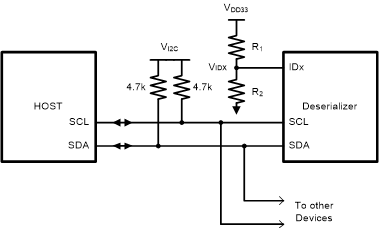
The device may also be configured by the use of a I2C-compatible serial control bus. Multiple devices may share the serial control bus (up to eight device addresses supported). The device address is set through a resistor divider (R1 and R2 — see Figure 33 below) connected to the IDx pin.
 Figure 33. Serial Control Bus Connection
 The serial control bus consists of two signals, SCL and SDA. SCL is a serial bus clock input. SDA is the serial bus data input / output signal. Both SCL and SDA signals require an external pullup resistor to 1.8-V or 3.3-V. For most applications, TI recommends that the user adds a 4.7-kΩ pullup resistor to the 3.3-V rail, however, the pullup resistor value may be adjusted for capacitive loading and data rate requirements. See I2C Bus Pullup Resistor Calculation (SLVA689) for more information. The signals are either pulled high or driven low.
The IDx pin configures the control interface to one of eight possible device addresses. A pullup resistor and a pulldown resistor may be used to set the appropriate voltage ratio between the IDx input pin (VR2) and VDD33, each ratio corresponding to a specific device address. See Table 10 for more information.
Table 10. Serial Control Bus Addresses for IDx
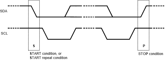
The serial bus protocol is controlled by START, START-Repeated, and STOP phases. A START occurs when SDA transitions low while SCL is high. A STOP occurs when SDA transitions high while SCL is also HIGH. See Figure 34.
 Figure 34. START and STOP Conditions
 To communicate with a remote device, the host controller (master) sends the slave address and listens for a response from the slave. This response is referred to as an acknowledge bit (ACK). If a slave on the bus is addressed correctly, it acknowledges (ACKs) the master by driving the SDA bus low. If the address does not match the slave address of a device, the slave not-acknowledges (NACKs) the master by letting the SDA be pulled High. ACKs also occur on the bus when data is transmitted. When the master writes data, the slave sends an ACK after every data byte is successfully received. When the master reads data, the master sends an ACK after every data byte is received to let the slave know that the master is ready to receive another data byte. When the master wants to stop reading, the master sends a NACK after the last data byte to create a stop condition on the bus. All communication on the bus begins with either a start condition or a repeated Start condition. All communication on the bus ends with a stop condition. A READ is shown in Figure 35 and a WRITE is shown in Figure 36.
 Figure 35. Serial Control Bus — READ
  Figure 36. Serial Control Bus — WRITE
 The I2C master located in the deserializer must support I2C clock stretching. For more information on I2C interface requirements and throughput considerations, refer to the I2C Communication Over FPD-Link III with Bidirectional Control Channel (SNLA131).