SBOS950A July 2019 – January 2021 INA253-Q1
PRODUCTION DATA
- 1 Features
- 2 Applications
- 3 Description
- 4 Revision History
- 5 Pin Configuration and Functions
- 6 Specifications
-
7 Detailed Description
- 7.1 Overview
- 7.2 Functional Block Diagram
- 7.3 Feature Description
- 7.4
Device Functional Modes
- 7.4.1 Adjusting the Output Midpoint With the Reference Pins
- 7.4.2 Reference Pin Connections for Unidirectional Current Measurements
- 7.4.3 Ground Referenced Output
- 7.4.4 Reference Pin Connections for Bidirectional Current Measurements
- 7.4.5 Output Set to Mid-Supply Voltage
- 7.4.6 Output Set to Mid-External Reference
- 7.4.7 Output Set Using Resistor Divide
- 8 Application and Implementation
- 9 Power Supply Recommendations
- 10Layout
- 11Device and Documentation Support
- 12Mechanical, Packaging, and Orderable Information
Package Options
Mechanical Data (Package|Pins)
- PW|20
Thermal pad, mechanical data (Package|Pins)
Orderable Information
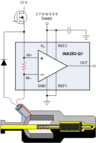
8.2.1 High-Side, High-Drive, Solenoid Current-Sense Application
Challenges exist in solenoid drive current sensing that are similar to those in motor inline current sensing. In certain topologies, the current-sensing amplifier is exposed to the full-scale PWM voltage between ground and supply. The INA253-Q1 is an excellent choice for this type of application. The 2-mΩ integrated shunt with a total system accuracy of 0.2% with a total system drift of 25 ppm/°C provides system accuracy across temperature eliminating the need for tri temperature system calibration.
 Figure 8-3 Solenoid Drive Application Circuit