SBOS950A July 2019 – January 2021 INA253-Q1
PRODUCTION DATA
- 1 Features
- 2 Applications
- 3 Description
- 4 Revision History
- 5 Pin Configuration and Functions
- 6 Specifications
-
7 Detailed Description
- 7.1 Overview
- 7.2 Functional Block Diagram
- 7.3 Feature Description
- 7.4
Device Functional Modes
- 7.4.1 Adjusting the Output Midpoint With the Reference Pins
- 7.4.2 Reference Pin Connections for Unidirectional Current Measurements
- 7.4.3 Ground Referenced Output
- 7.4.4 Reference Pin Connections for Bidirectional Current Measurements
- 7.4.5 Output Set to Mid-Supply Voltage
- 7.4.6 Output Set to Mid-External Reference
- 7.4.7 Output Set Using Resistor Divide
- 8 Application and Implementation
- 9 Power Supply Recommendations
- 10Layout
- 11Device and Documentation Support
- 12Mechanical, Packaging, and Orderable Information
Package Options
Mechanical Data (Package|Pins)
- PW|20
Thermal pad, mechanical data (Package|Pins)
Orderable Information
7.4.1 Adjusting the Output Midpoint With the Reference Pins
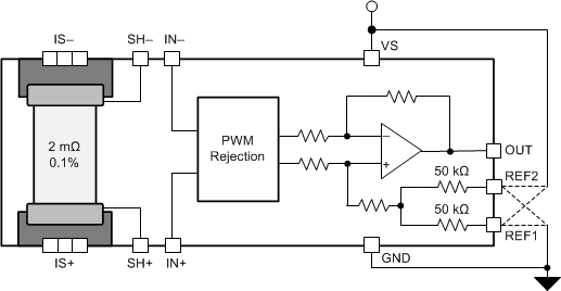
Figure 7-5 shows a test circuit for reference-divider accuracy. The INA253-Q1 output is configurable to allow for unidirectional or bidirectional operation.
CAUTION:
Do not connect the REF1 pin or the REF2 pin to any voltage source lower than GND or higher than VS.
The output voltage is set by applying a voltage or voltages to the reference voltage inputs, REF1 and REF2. The reference inputs are connected to an internal gain network. There is no operational difference between the two reference pins.
 Figure 7-5 Adjusting the Output Midpoint