SBOS977A March 2019 – May 2021 INA302-Q1 , INA303-Q1
PRODUCTION DATA
- 1 Features
- 2 Applications
- 3 Description
- 4 Revision History
- 5 Pin Configuration and Functions
- 6 Specifications
- 7 Detailed Description
- 8 Application and Implementation
- 9 Power Supply Recommendations
- 10Layout
- 11Device and Documentation Support
- 12Mechanical, Packaging, and Orderable Information
Package Options
Mechanical Data (Package|Pins)
- PW|14
Thermal pad, mechanical data (Package|Pins)
Orderable Information
6.6 Typical Characteristics
at TA = 25°C, VREF = VS / 2, VSENSE = 0 V, VS = 5 V, VIN+ = 12 V, and ALERT1, ALERT2 pullup resistors = 10 kΩ (unless otherwise noted)
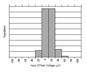 Figure 6-1 Input Offset Voltage Distribution (INA30xA1-Q1)
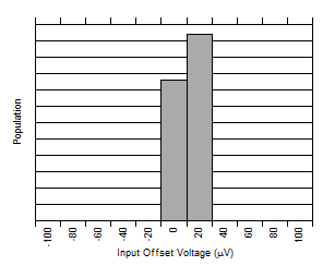 Figure 6-3 Input Offset Voltage Distribution (INA30xA3-Q1)
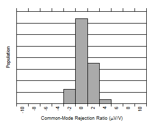 Figure 6-5 CMRR Distribution (INA30xA1-Q1)
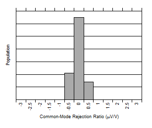 Figure 6-7 CMRR Distribution (INA30xA3-Q1)
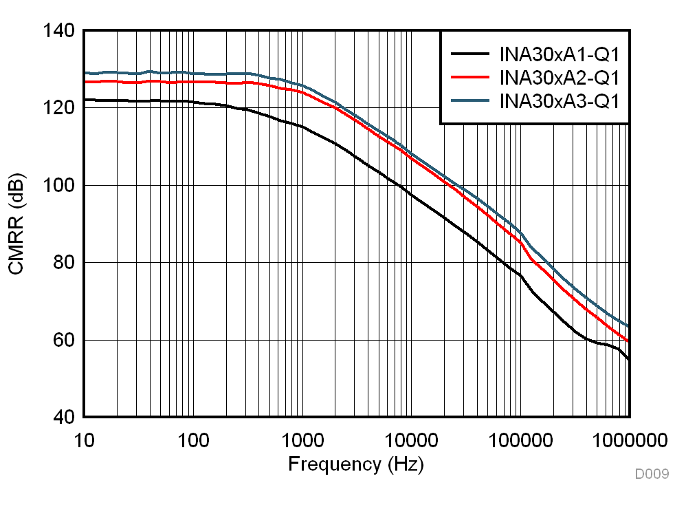 Figure 6-9 CMRR vs.
Frequency
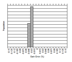 Figure 6-11 Gain Error Distribution (INA30xA2-Q1)
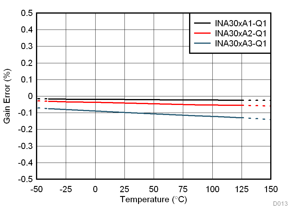 Figure 6-13 Gain Error vs.
Temperature
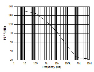 Figure 6-15 PSRR vs.
Frequency
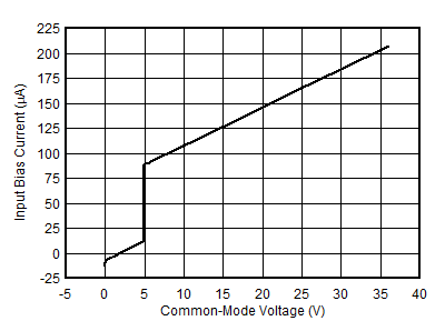
| VS = 5 V | ||
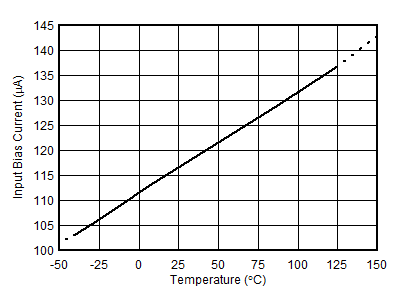 Figure 6-19 Input Bias Current vs.
Temperature
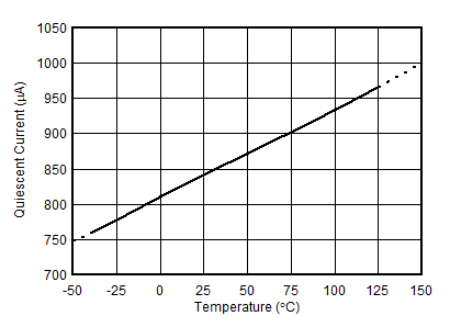 Figure 6-21 Quiescent Current vs.
Temperature
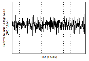
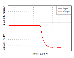
| 4-VPP output step | ||
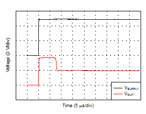 Figure 6-27 Start-Up Response
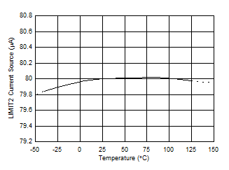 Figure 6-29 LIMIT2 Current Source vs.
Temperature
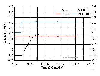 Figure 6-31 Comparator 1 Total Propagation Delay (INA30x-Q1)
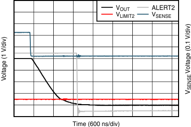
| DELAY = 100 kΩ to VS | ||
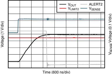
| DELAY = 100 kΩ to VS | ||
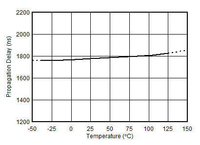
| VOD = 1 mV | ||
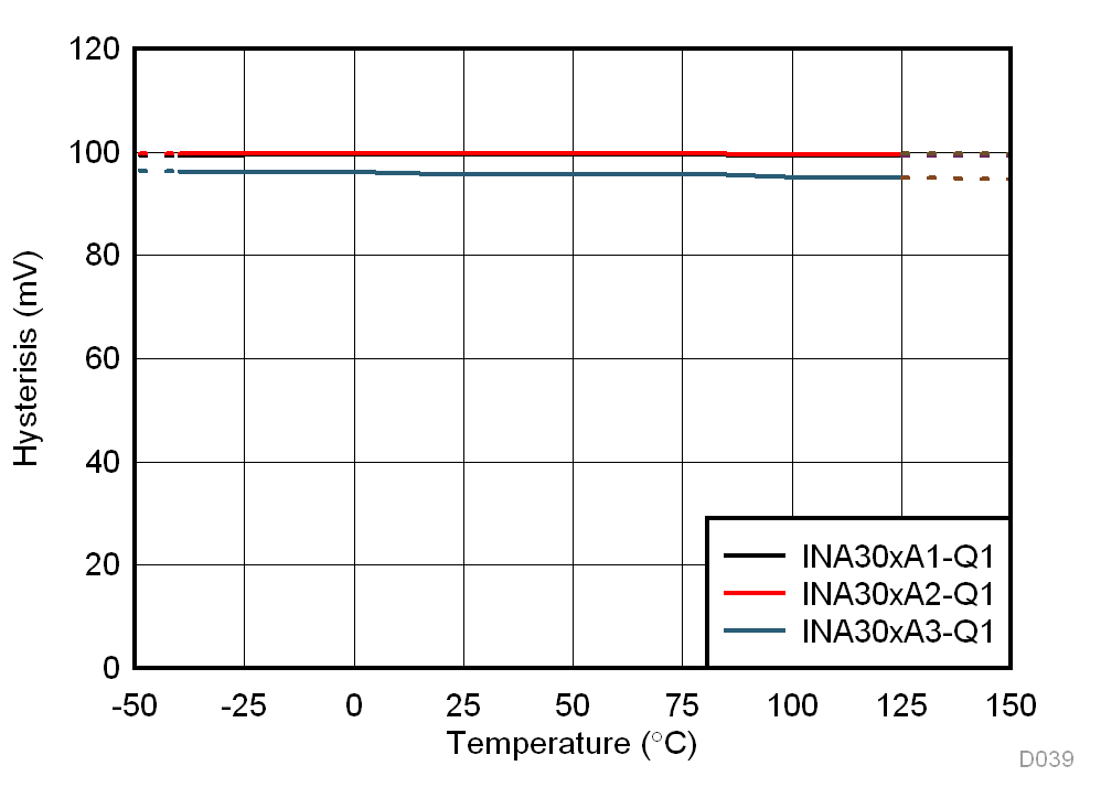 Figure 6-39 Comparator 1 Hysteresis
vs. Temperature
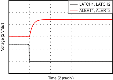 Figure 6-41 Comparator Latch Response
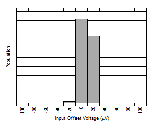 Figure 6-2 Input Offset Voltage Distribution (INA30xA2-Q1)
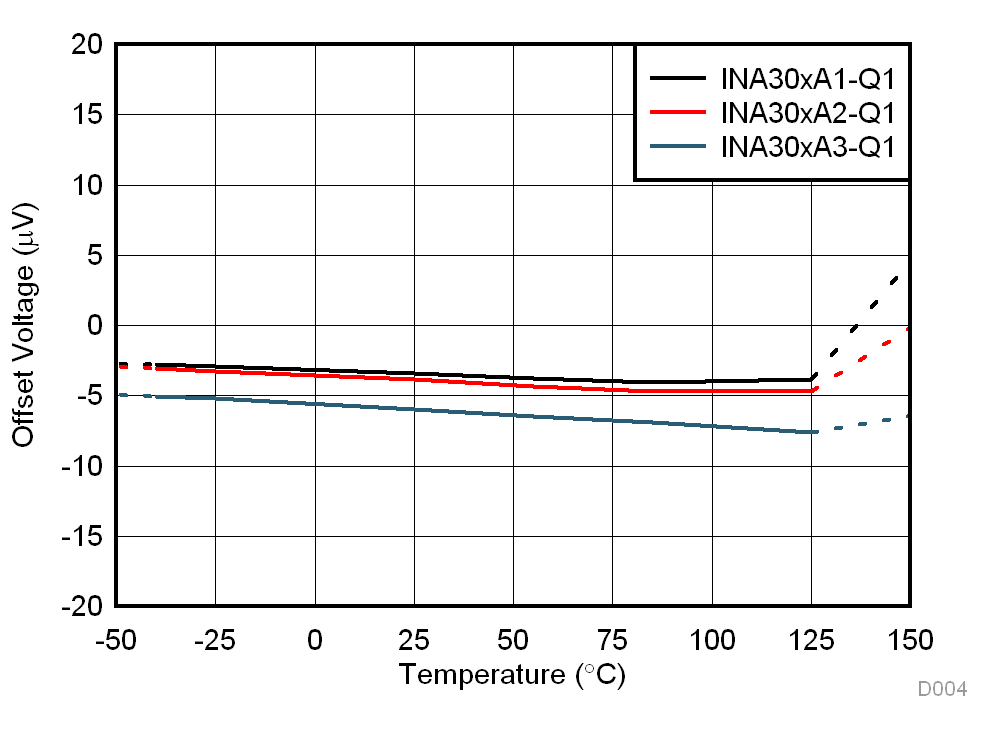 Figure 6-4 Input Offset Voltage vs.
Temperature
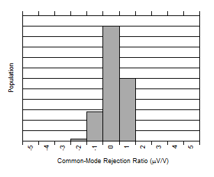 Figure 6-6 CMRR Distribution (INA30xA2-Q1)
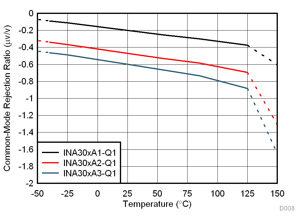 Figure 6-8 CMRR vs.
Temperature
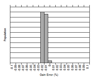 Figure 6-10 Gain Error Distribution (INA30xA1-Q1)
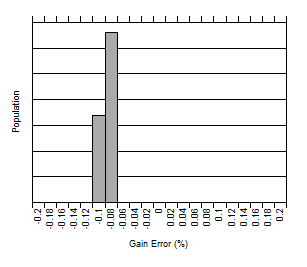 Figure 6-12 Gain Error Distribution (INA30xA3-Q1)
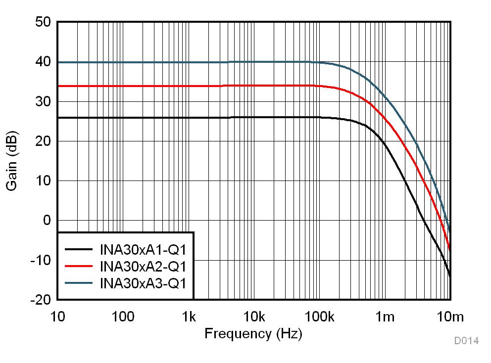 Figure 6-14 Gain vs.
Frequency
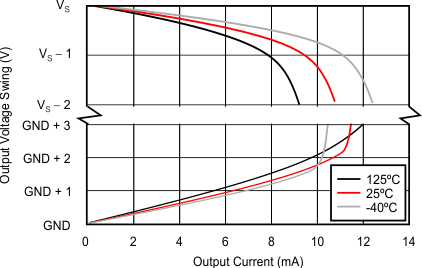 Figure 6-16 Output Voltage Swing vs.
Output Current
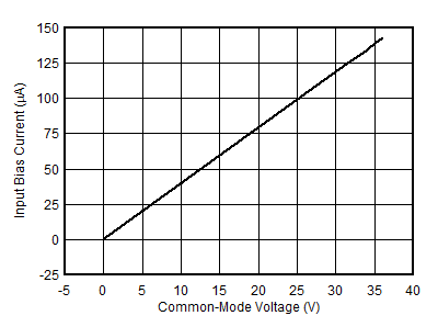
| VS = 0 V | ||
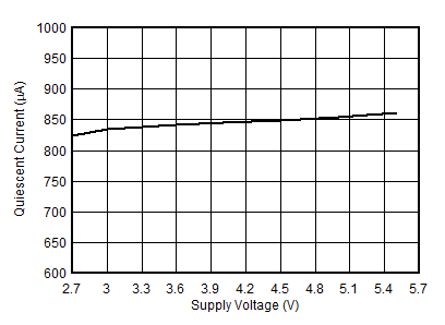 Figure 6-20 Quiescent Current vs.
Supply Voltage
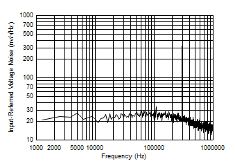 Figure 6-22 Input-Referred Voltage
Noise vs. Frequency
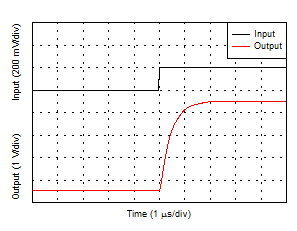
| 4-VPP output step | ||
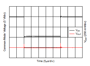 Figure 6-26 Common-Mode Voltage Transient Response
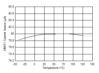 Figure 6-28 LIMIT1 Current Source vs.
Temperature
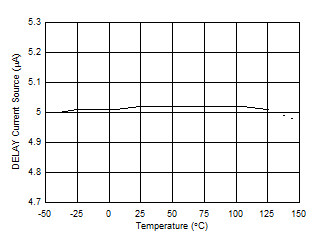 Figure 6-30 DELAY Current vs.
Temperature
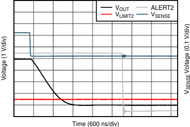
| DELAY = open | ||
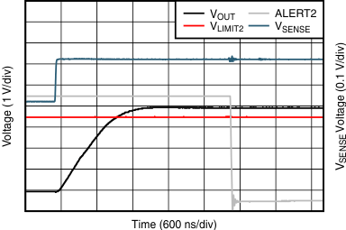
| DELAY = open | ||
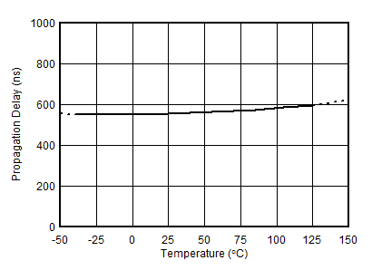
| VOD = 1 mV |
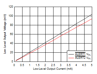 Figure 6-38 Comparator Alert
VOL vs. IOL
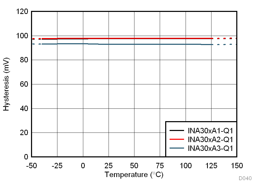 Figure 6-40 Comparator 2 Hysteresis
vs. Temperature
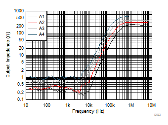 Figure 6-42 Output Impedance vs.
Frequency