SBOS776C March 2016 – March 2021 INA3221-Q1
PRODUCTION DATA
- 1 Features
- 2 Applications
- 3 Description
- 4 Revision History
- 5 Device Comparison Table
- 6 Pin Configuration and Functions
- 7 Specifications
-
8 Detailed Description
- 8.1 Overview
- 8.2 Functional Block Diagram
- 8.3 Feature Description
- 8.4 Device Functional Modes
- 8.5 Programming
- 8.6
Register Maps
- 8.6.1 Summary of Register Set
- 8.6.2
Register Descriptions
- 8.6.2.1 Configuration Register (address = 00h) [reset = 7127h]
- 8.6.2.2 Channel-1 Shunt-Voltage Register (address = 01h), [reset = 00h]
- 8.6.2.3 Channel-1 Bus-Voltage Register (address = 02h) [reset = 00h]
- 8.6.2.4 Channel-2 Shunt-Voltage Register (address = 03h) [reset = 00h]
- 8.6.2.5 Channel-2 Bus-Voltage Register (address = 04h) [reset = 00h]
- 8.6.2.6 Channel-3 Shunt-Voltage Register (address = 05h) [reset = 00h]
- 8.6.2.7 Channel-3 Bus-Voltage Register (address = 06h) [reset = 00h]
- 8.6.2.8 Channel-1 Critical-Alert Limit Register (address = 07h) [reset = 7FF8h]
- 8.6.2.9 Warning-Alert Channel-1 Limit Register (address = 08h) [reset = 7FF8h]
- 8.6.2.10 Channel-2 Critical-Alert Limit Register (address = 09h) [reset = 7FF8h]
- 8.6.2.11 Channel-2 Warning-Alert Limit Register (address = 0Ah) [reset = 7FF8h]
- 8.6.2.12 Channel-3 Critical-Alert Limit Register (address = 0Bh) [reset = 7FF8h]
- 8.6.2.13 Channel-3 Warning-Alert Limit Register (address = 0Ch) [reset = 7FF8h]
- 8.6.2.14 Shunt-Voltage Sum Register (address = 0Dh) [reset = 00h]
- 8.6.2.15 Shunt-Voltage Sum-Limit Register (address = 0Eh) [reset = 7FFEh]
- 8.6.2.16 Mask/Enable Register (address = 0Fh) [reset = 0002h]
- 8.6.2.17 Power-Valid Upper-Limit Register (address = 10h) [reset = 2710h]
- 8.6.2.18 Power-Valid Lower-Limit Register (address = 11h) [reset = 2328h]
- 8.6.2.19 Manufacturer ID Register (address = FEh) [reset = 5449h]
- 8.6.2.20 Die ID Register (address = FFh) [reset = 3220]
- 9 Application and Implementation
- 10Power Supply Recommendations
- 11Layout
- 12Device and Documentation Support
- 13Mechanical, Packaging, and Orderable Information
Package Options
Mechanical Data (Package|Pins)
- RGV|16
Thermal pad, mechanical data (Package|Pins)
Orderable Information
8.3.2.4 Timing-Control Alert
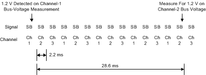
The INA3221-Q1 timing-control alert function helps verify proper power-supply sequencing. At power-up, the default INA3221-Q1 setting is continuous shunt- and bus-voltage conversion mode, and the INA3221-Q1 internally begins comparing the channel-1 bus voltage to determine when a 1.2-V level is reached. This comparison is made each time the sequence returns to the channel-1 bus-voltage measurement. When a 1.2-V level is detected on the channel-1 bus-voltage measurement, the INA3221-Q1 begins checking for a 1.2-V level present on the channel-2 bus-voltage measurement. After a 1.2-V level is detected on channel 1, if the INA3221-Q1 does not detect a 1.2-V value or greater on the bus voltage measurement following four complete cycles of all three channels, the timing control (TC) alert pin pulls low to indicate that the INA3221-Q1 has not detected a valid power rail on channel 2. As shown in Figure 8-3, this sequence allows for approximately 28.6 ms from the time 1.2 V is detected on channel 1 for a valid voltage to be detected on channel 2. Figure 8-4 illustrates the state diagram for the TC alert pin.

 Figure 8-4 Timing Control State Diagram
The timing control alert function is only monitored at power-up or when a software reset is issued by setting the reset bit (RST, bit 15) in the Configuration register. The timing control alert function timing is based on the default device settings at power-up. Writing to the Configuration register before the timing control alert function completes the full sequence results in disabling the timing control alert until power is cycled or a software reset is issued.