SLLS897F march 2008 – august 2023 ISO1176
PRODUCTION DATA
- 1
- 1 Features
- 2 Applications
- 3 Description
- 4 Revision History
- 5 Pin Configuration and Functions
-
6 Specifications
- 6.1 Absolute Maximum Ratings
- 6.2 ESD Ratings
- 6.3 Recommended Operating Conditions
- 6.4 Thermal Information
- 6.5 Power Ratings
- 6.6 Insulation Specifications
- 6.7 Safety-Related Certifications
- 6.8 Safety Limiting Values
- 6.9 Electrical Characteristics: Driver
- 6.10 Electrical Characteristics: Receiver
- 6.11 Supply Current
- 6.12 Electrical Characteristics: ISODE-Pin
- 6.13 Switching Characteristics: Driver
- 6.14 Switching Characteristics: Receiver
- 6.15 Insulation Characteristics Curves
- 6.16 Typical Characteristics
- 7 Parameter Measurement Information
- 8 Detailed Description
- 9 Application and Implementation
- 10Power Supply Recommendations
- 11Layout
- 12Device and Documentation Support
- 13Mechanical, Packaging, and Orderable Information
Package Options
Mechanical Data (Package|Pins)
- DW|16
Thermal pad, mechanical data (Package|Pins)
- DW|16
Orderable Information
9.2.2.1 Transient Voltages
From this model, the voltage at the isolated bus return is
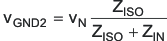
and is always less than 16 V from VN. If the ISO1176 is tested as a stand-alone device,
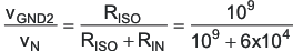
- RIN= 6 x 10⁴ Ω,
- CIN= 16 x 10–12 F,
- RISO= 109 Ω and
- CISO= 10–12 F.
Notice from Figure 9-2 that the resistor ratio determines the voltage ratio at low frequencies, and that the inverse capacitance ratio determines the voltage ration at high frequencies. In the stand-alone case and for low frequencies,
or essentially all of the noise appears across the barrier.
At high frequencies,
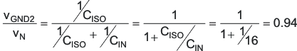
and 94% of VN appears across the barrier. As long as RISO is greater than RIN and CISO is less than CIN, most of the transient noise appears across the isolation barrier, as it should.
Using ESD generators to test equipment transient susceptibility, or considering product claims of ESD ratings greater than the barrier transient ratings of an isolated interface is not recommended. ESD is best managed through recessing or covering connector pins in a conductive connector shell, and by proper installer training.