SLLSFC5D November 2021 – April 2025 ISOUSB211
PRODUCTION DATA
- 1
- 1 Features
- 2 Applications
- 3 Description
- 4 Pin Configuration and Functions
-
5 Specifications
- 5.1 Absolute Maximum Ratings
- 5.2 ESD Ratings
- 5.3 Recommended Operating Conditions
- 5.4 Thermal Information
- 5.5 Power Ratings
- 5.6 Insulation Specifications
- 5.7 Safety-Related Certifications
- 5.8 Safety Limiting Values
- 5.9 Electrical Characteristics
- 5.10 Switching Characteristics
- 5.11 Insulation Characteristics Curves
- 5.12 Typical Characteristics
- 6 Parameter Measurement Information
-
7 Detailed Description
- 7.1 Overview
- 7.2 Functional Block Diagram
- 7.3
Feature Description
- 7.3.1 Power Supply Options
- 7.3.2 Power Up
- 7.3.3 Symmetric Operation, Dual-Role Port, and Role-Reversal
- 7.3.4 Connect and Speed Detection
- 7.3.5 Disconnect Detection
- 7.3.6 Reset
- 7.3.7 LS/FS Message Traffic
- 7.3.8 HS Message Traffic
- 7.3.9 Equalization and Pre-emphasis
- 7.3.10 L2 Power Management State (Suspend) and Resume
- 7.3.11 L1 Power Management State (Sleep) and Resume
- 7.3.12 HS Test Mode Support
- 7.3.13 CDP Advertising
- 7.4 Device Functional Modes
- 8 Application and Implementation
- 9 Device and Documentation Support
- 10Revision History
- 11Mechanical, Packaging, and Orderable Information
Package Options
Mechanical Data (Package|Pins)
- DP|28
Thermal pad, mechanical data (Package|Pins)
Orderable Information
8.1.1 Isolated Host or Hub
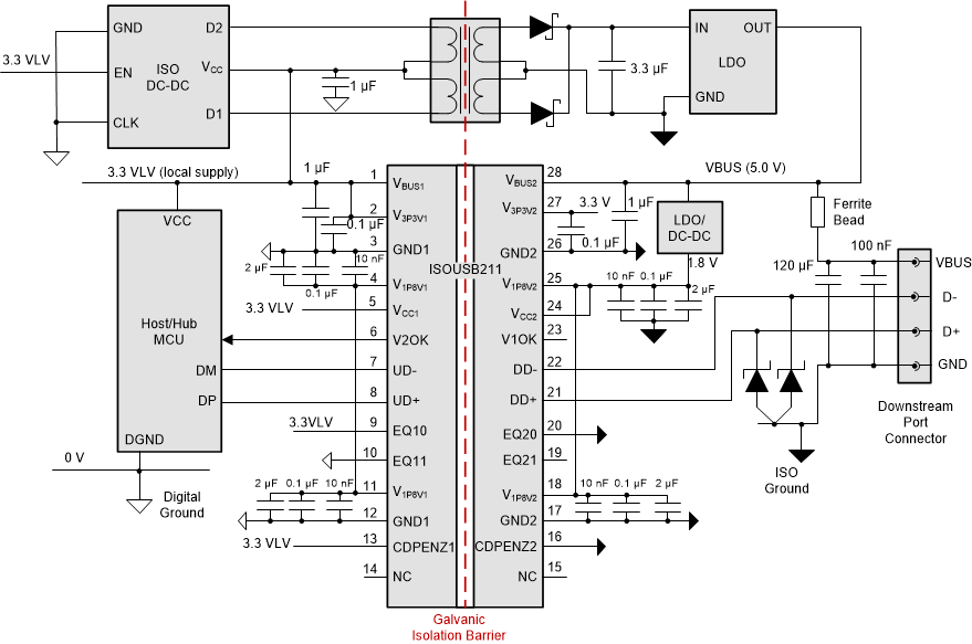
Figure 8-1 shows an application for isolating a host or a hub using ISOUSB211. In this example, on the microcontrollers side, V3P3V1 and VBUS1 are together connected to an external 3.3-V supply. The V1P8V1 supply is generated using the internal 1.8-V LDO by providing 3.3-V supply to VCC1. On the connector side, the VBUS from the USB connector is connected to VBUS2 and the V3P3V2 supply is generated using the internal 3.3-V LDO. VCC2 and V1P8V2 are together connected to an external 1.8-V supply derived from VBUS. Please refer to Thermal Considerations for options on optimizing power dissipation inside ISOUSB211 as required.
Decoupling capacitors are placed next to ISOUSB211 according to the recommendations provided in the Power Supply Recommendations section. An isolated DC-DC converter (such as the SN6505) is to provide power to the VBUS using the 3.3-V local supply. Note that, for a host or hub, the USB standard requires a 120-μF capacitor to be placed on the VBUS so as to be able provide in-rush current when a downstream peripheral is attached. In addition, a 100-nF capacitor is recommended close to the VBUS pin to handle transient currents.
ESD diodes with low capacitance and low dynamic resistance, such as PESD5V0C1USF, can be placed on D+ and D- lines. A ferrite bead, with DC resistance less than 100 mΩ, can be optionally placed between VBUS pin of the connector and the VBUS pin of ISOUSB211, as shown in the figure, to suppress transients such as ESD.
If the isolated power supply used is capable of providing >1.5 A current on the VBUS, the port can be configured as a CDP port according to Battery Charger specification BC 1.2. To make this configuration this, the CDPENZ2 pin of ISOUSB211 must be connected to ground as shown. Under this condition ISOUSB211 responds to BC 1.2 signaling from a connected peripheral indicating to the peripheral that the port is capable of supply 1.5-A current on VBUS.
 Figure 8-1 Isolated Host
or Hub With ISOUSB211