SNOSDC7B December 2021 – December 2021 LDC3114-Q1
PRODUCTION DATA
- 1 Features
- 2 Applications
- 3 Description
- 4 Revision History
- 5 Pin Configuration and Functions
- 6 Specifications
-
7 Detailed Description
- 7.1 Overview
- 7.2 Functional Block Diagram
- 7.3 Feature Description
- 7.4 Device Functional Modes
- 7.5 Register Maps
-
8 Application and Implementation
- 8.1
Application Information
- 8.1.1 Theory of Operation
- 8.1.2 Designing Sensor Parameters
- 8.1.3 Setting COM Pin Capacitor
- 8.1.4 Defining Power-On Timing
- 8.1.5 Configuring Button or Raw Data Scan Rate
- 8.1.6 Programming Button or Raw Data Sampling Window
- 8.1.7 Scaling Frequency Counter Output
- 8.1.8 Setting Button Triggering Threshold
- 8.1.9 Tracking Baseline
- 8.1.10 Mitigating False Button Detections
- 8.1.11 Reporting Interrupts for Button Presses, Raw Data Ready and Error Conditions
- 8.1.12 Estimating Supply Current
- 8.2 Typical Application
- 8.1
Application Information
- 9 Power Supply Recommendations
- 10Layout
- 11Device and Documentation Support
- 12Mechanical, Packaging, and Orderable Information
Package Options
Mechanical Data (Package|Pins)
- PW|16
Thermal pad, mechanical data (Package|Pins)
Orderable Information
3 Description
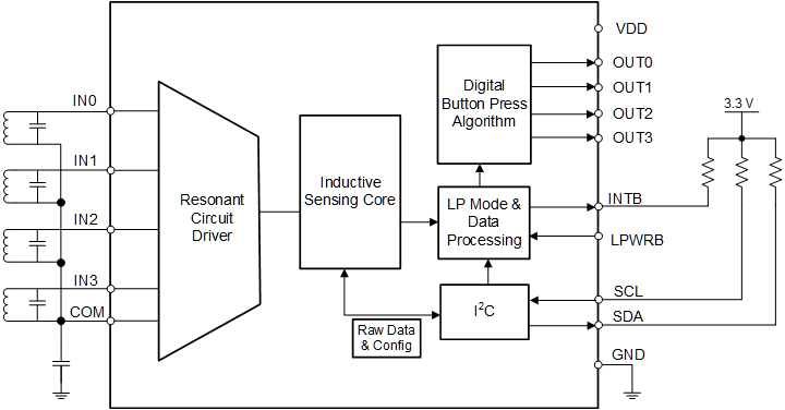
The LDC3114-Q1 is an inductive sensing device that enables touch button design for human machine interface (HMI) on a wide variety of materials by measuring small deflections of conductive targets using a coil that can be implemented on a small printed circuit board (PCB) located behind the panel. This technology can be used for precise linear position sensing of metal targets for automotive, consumer and industrial applications by allowing access to the raw data representing the inductance value. Inductive sensing solution is insensitive to humidity or non-conductive contaminants such as oil and dirt.
The button mode of LDC3114-Q1 is able to automatically correct for any deformation in the conductive targets. The LDC3114-Q1 offers well-matched channels, which allow for differential and ratiometric measurements which enable compensation of environmental and aging conditions such as temperature and mechanical drift. The LDC3114-Q1 includes an ultra-low power mode intended for power on/off buttons or position sensors in battery powered applications.
The LDC3114-Q1 is easily configured through an I2C interface. The LDC3114-Q1 is available in a 16-pin TSSOP package.
| PART NUMBER | PACKAGE | BODY SIZE (NOM) |
|---|---|---|
| LDC3114-Q1 | TSSOP (16) | 5.00 mm × 4.40 mm |
 LDC3114-Q1 Simplified
Schematic