SNVS585M September 2008 – October 2020 LM22678 , LM22678-Q1
PRODUCTION DATA
- 1 Features
- 2 Applications
- 3 Description
- 4 Revision History
- 5 Pin Configuration and Functions
- 6 Specifications
- 7 Detailed Description
- 8 Application and Implementation
- 9 Layout
- 10Device and Documentation Support
Package Options
Mechanical Data (Package|Pins)
- NDR|7
Thermal pad, mechanical data (Package|Pins)
Orderable Information
7.3.1 Precision Enable and UVLO
The precision enable input (EN) is used to control the regulator. The precision feature allows simple sequencing of multiple power supplies with a resistor divider from another supply. Connecting this pin to ground or to a voltage less than 1.6 V (typ.) will turn off the regulator. The current drain from the input supply, in this state, is 25 µA (typ.) at an input voltage of 12 V. The EN input has an internal pullup of about 6 µA. Therefore, this pin can be left floating or pulled to a voltage greater than 2.2 V (typ) to turn the regulator on. The hysteresis on this input is about 0.6 V (typ.) above the 1.6-V (typ.) threshold. When driving the enable input, the voltage must never exceed the 6-V absolute maximum specification for this pin.
Although an internal pullup is provided on the EN pin, it is good practice to pull the input high when this feature is not used, especially in noisy environments. This can most easily be done by connecting a resistor between VIN and the EN pin. The resistor is required because the internal zener diode at the EN pin will conduct for voltages above about 6 V. The current in this zener must be limited to less than 100 µA. A resistor of 470 kΩ will limit the current to a safe value for input voltages as high 42 V. Smaller values of resistor can be used at lower input voltages.
The LM22678 device also incorporates an input undervoltage lockout (UVLO) feature. This prevents the regulator from turning on when the input voltage is not great enough to properly bias the internal circuitry. The rising threshold is 4.3 V (typ.) while the falling threshold is 3.9 V (typ.). In some cases, these thresholds can be too low to provide good system performance. The solution is to use the EN input as an external UVLO to disable the part when the input voltage falls below a lower boundary. This is often used to prevent excessive battery discharge or early turnon during start-up. This method is also recommended to prevent abnormal device operation in applications where the input voltage falls below the minimum of 4.5 V. Figure 7-1 shows the connections to implement this method of UVLO. Equation 1 and Equation 2 can be used to determine the correct resistor values.
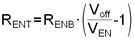
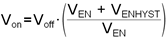
where
- Voff is the input voltage where the regulator shuts off.
- Von is the voltage where the regulator turns on.
Due to the 6-µA pullup, the current in the divider should be much larger than this. A value of 20 kΩ, for RENB is a good first choice. Also, a zener diode may be needed between the EN pin and ground, in order to comply with the absolute maximum ratings on this pin.
 Figure 7-1 External UVLO Connections