SNVS581M February 2013 – October 2020 LM22679 , LM22679-Q1
PRODUCTION DATA
- 1 Features
- 2 Applications
- 3 Description
- 4 Revision History
- 5 Pin Configuration and Functions
- 6 Specifications
- 7 Detailed Description
- 8 Application and Implementation
- 9 Power Supply Recommendations
- 10Layout
- 11Device and Documentation Support
Package Options
Mechanical Data (Package|Pins)
- NDR|7
Thermal pad, mechanical data (Package|Pins)
Orderable Information
8.2.1.2.3 Input Capacitor
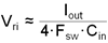
The input capacitor selection is based on both input voltage ripple and RMS current. Good quality input capacitors are necessary to limit the ripple voltage at the VIN pin while supplying most of the regulator current during switch on-time. Low-ESR ceramic capacitors are preferred. Larger values of input capacitance are desirable to reduce voltage ripple and noise on the input supply. This noise may find its way into other circuitry, sharing the same input supply, unless adequate bypassing is provided. A very approximate formula for determining the input voltage ripple is shown in Equation 13.
where
- Vri is the peak-to-peak ripple voltage at the switching frequency
Another concern is the RMS current passing through this capacitor. Equation 14 determines an approximation to this current.

The capacitor must be rated for at least this level of RMS current at the switching frequency.
All ceramic capacitors have large voltage coefficients, in addition to normal tolerances and temperature coefficients. To help mitigate these effects, multiple capacitors can be used in parallel to bring the minimum capacitance up to the desired value. This may also help with RMS current constraints by sharing the current among several capacitors. Many times it is desirable to use an electrolytic capacitor on the input, in parallel with the ceramics. The moderate ESR of this capacitor can help to damp any ringing on the input supply caused by long power leads. This method can also help to reduce voltage spikes that can exceed the maximum input voltage rating of the LM22679.
It is good practice to include a high frequency bypass capacitor as close as possible to the LM22679. This small case size, low ESR, ceramic capacitor should be connected directly to the VIN and GND pins with the shortest possible PCB traces. Values in the range of 0.47 µF to 1 µF are appropriate. This capacitor helps to provide a low impedance supply to sensitive internal circuitry. It also helps to suppress any fast noise spikes on the input supply that can lead to increased EMI.