SNVS581M February 2013 – October 2020 LM22679 , LM22679-Q1
PRODUCTION DATA
- 1 Features
- 2 Applications
- 3 Description
- 4 Revision History
- 5 Pin Configuration and Functions
- 6 Specifications
- 7 Detailed Description
- 8 Application and Implementation
- 9 Power Supply Recommendations
- 10Layout
- 11Device and Documentation Support
Package Options
Mechanical Data (Package|Pins)
- NDR|7
Thermal pad, mechanical data (Package|Pins)
Orderable Information
7.4.4 Current Limit Adjustment
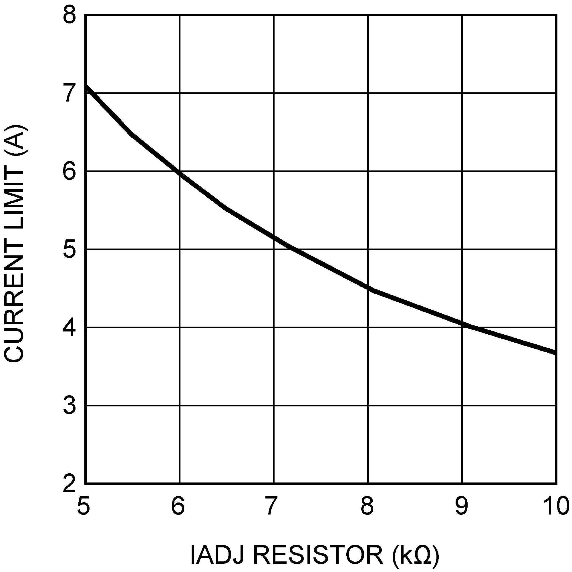
A key feature of the LM22679 device is the ability to adjust the peak switch current limit. This can be useful when the full current capability of the regulator is not required for a given application. A smaller current limit may allow the use of power components with lower current ratings, thus saving space and reducing cost. A single resistor between the IADJ pin and ground controls the current limit in accordance with Figure 7-3. The current limit mode is set during start-up of the regulator. When VIN is applied, a weak pullup is connected to the IADJ pin and, after approximately 100 µs, the voltage on the pin is checked against a threshold of about 0.8 V. With the IADJ pin open, the voltage floats above this threshold, and the current limit is set to the default value of 7.1 A (typ). With a resistor present, an internal reference holds the pin voltage at 0.8 V; thus, the resulting current sets the current limit. The accuracy of the adjusted current limit will be slightly worse than that of the default value; +35% / –25% is to be expected. Resistor values should not exceed the limits shown in Figure 7-3.
 Figure 7-3 Current Limit vs IADJ Resistor