SNVS859C July 2012 – September 2016 LM25101
PRODUCTION DATA.
- 1 Features
- 2 Applications
- 3 Description
- 4 Revision History
- 5 Device Options
- 6 Pin Configuration and Functions
- 7 Specifications
- 8 Detailed Description
- 9 Application and Implementation
- 10Power Supply Recommendations
- 11Layout
- 12Device and Documentation Support
- 13Mechanical, Packaging, and Orderable Information
Package Options
Mechanical Data (Package|Pins)
Thermal pad, mechanical data (Package|Pins)
Orderable Information
8 Detailed Description
8.1 Overview
To operate fast switching of power MOSFETs at high switching frequencies and to reduce associated switching losses, a powerful gate driver is employed between the PWM output of controller and the gates of the power semiconductor devices. Also, gate drivers are indispensable when it is impossible for the PWM controller to directly drive the gates of the switching devices. With the advent of digital power, this situation is often encountered because the PWM signal from the digital controller is often a 3.3 V logic signal which cannot effectively turn on a power switch. Level shift circuitry is needed to boost the 3.3-V signal to the gate-drive voltage (such as 12 V) in order to fully turn on the power device and minimize conduction losses. Traditional buffer drive circuits based on NPN or PNP bipolar transistors in totem-pole arrangement prove inadequate with digital power because they lack level-shifting capability. Gate drivers effectively combine both the level-shifting and buffer-drive functions. Gate drivers also find other needs such as minimizing the effect of high-frequency switching noise (by placing the high-current driver IC physically close to the power switch), driving gate-drive transformers and controlling floating power-device gates, reducing power dissipation and thermal stress in controllers by moving gate charge power losses from the controller into the driver.
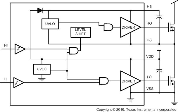
8.2 Functional Block Diagram

8.3 Feature Description
8.3.1 Start-Up and UVLO
Both top and bottom drivers include UVLO protection circuitry which monitors the supply voltage (VDD) and bootstrap capacitor voltage (VHB-HS) independently. The UVLO circuit inhibits each output until sufficient supply voltage is available to turn on the external MOSFETs, and the built-in UVLO hysteresis prevents chattering during supply voltage variations. When the supply voltage is applied to the VDD pin of the LM25101, the top and bottom gates are held low until VDD exceeds the UVLO threshold, typically about 6.9 V. Any UVLO condition on the bootstrap capacitor (VHB-HS) will only disable the high-side output (HO).
Table 2. VDD UVLO Feature Logic Operation
| CONDITION(1) | HI | LI | HO | LO |
|---|---|---|---|---|
| VDD – VSS < VDDR during device start-up | H | L | L | L |
| VDD – VSS < VDDR during device start-up | L | H | L | L |
| VDD – VSS < VDDR during device start-up | H | H | L | L |
| VDD – VSS < VDDR during device start-up | L | L | L | L |
| VDD – VSS < VDDR – VDDH after device start-up | H | L | L | L |
| VDD – VSS < VDDR – VDDH after device start-up | L | H | L | L |
| VDD – VSS < VDDR – VDDH after device start-up | H | H | L | L |
| VDD – VSS < VDDR – VDDH after device start-up | L | L | L | L |
Table 3. VHB-HS UVLO Feature Logic Operation
| CONDITION(1) | HI | LI | HO | LO |
|---|---|---|---|---|
| VHB→HS < VHBR during device start-up | H | L | L | L |
| VHB–HS < VHBR during device start-up | L | H | L | H |
| VHB–HS < VHBR during device start-up | H | H | L | H |
| VHB–HS < VHBR during device start-up | L | L | L | L |
| VHB–HS < VHBR – VHBH after device start-up | H | L | L | L |
| VHB–HS < VHBR – VHBH after device start-up | L | H | L | H |
| VHB–HS < VHBR – VHBH after device start-up | H | H | L | H |
| VHB–HS < VHBR – VHBH after device start-up | L | L | L | L |
8.3.2 Level Shift
The level shift circuit is the interface from the high-side input to the high-side driver stage which is referenced to the switch node (HS). The level shift allows control of the HO output which is referenced to the HS pin and provides excellent delay matching with the low-side driver.
8.3.3 Output Stages
The output stages are the interface to the power MOSFETs in the power train. High slew rate, low resistance, and high peak current capability of both outputs allow for efficient switching of the power MOSFETs. The low-side output stage is referenced to VSS and the high-side is referenced to HS.
8.4 Device Functional Modes
The device operates in normal mode and UVLO mode. See Start-Up and UVLO for more information on UVLO operation mode. In normal mode when the VDD and VHB–HS are above UVLO threshold, the output stage is dependent on the states of the HI and LI pins. Unused inputs should be tied to ground and not left open.