SNVS726F July   2011  – March 2018 LM25118

PRODUCTION DATA.  

  1. Features
  2. Applications
  3. Description
    1.     Device Images
      1.      Simplified Schematic
      2.      Efficiency vs VIN and IOUT, VOUT = 12 V
  4. Revision History
  5. Pin Configuration and Functions
    1.     Pin Functions
  6. Specifications
    1. 6.1 Absolute Maximum Ratings
    2. 6.2 ESD Ratings
    3. 6.3 Recommended Operating Conditions
    4. 6.4 Thermal Information
    5. 6.5 Electrical Characteristics
    6. 6.6 Typical Characteristics
  7. Detailed Description
    1. 7.1 Overview
    2. 7.2 Functional Block Diagram
    3. 7.3 Feature Description
      1. 7.3.1 UVLO
      2. 7.3.2 Oscillator and Sync Capability
      3. 7.3.3 Error Amplifier and PWM Comparator
      4. 7.3.4 Ramp Generator
      5. 7.3.5 Current Limit
      6. 7.3.6 Maximum Duty Cycle
      7. 7.3.7 Soft Start
      8. 7.3.8 HO Output
      9. 7.3.9 Thermal Protection
    4. 7.4 Device Functional Modes
      1. 7.4.1 Buck Mode Operation: VIN > VOUT
      2. 7.4.2 Buck-Boost Mode Operation: VIN ≊ VOUT
      3. 7.4.3 High Voltage Start-Up Regulator
      4. 7.4.4 Enable
  8. Application and Implementation
    1. 8.1 Application Information
    2. 8.2 Typical Application
      1. 8.2.1 Design Requirements
      2. 8.2.2 Detailed Design Procedure
        1. 8.2.2.1  Custom Design With WEBENCH® Tools
        2. 8.2.2.2  R7 = RT
        3. 8.2.2.3  Inductor Selection – L1
        4. 8.2.2.4  R13 = RSENSE
        5. 8.2.2.5  C15 = CRAMP
        6. 8.2.2.6  Inductor Current Limit Calculation
        7. 8.2.2.7  C9 - C12 = Output Capacitors
        8. 8.2.2.8  D1
        9. 8.2.2.9  D4
        10. 8.2.2.10 C1 – C5 = Input Capacitors
        11. 8.2.2.11 C20
        12. 8.2.2.12 C8
        13. 8.2.2.13 C16 = CSS
        14. 8.2.2.14 R8, R9
        15. 8.2.2.15 R1, R3, C21
        16. 8.2.2.16 R2
        17. 8.2.2.17 Snubber
        18. 8.2.2.18 Error Amplifier Configuration
          1. 8.2.2.18.1 R4, C18, C17
      3. 8.2.3 Application Curves
  9. Power Supply Recommendations
    1. 9.1 Bias Power Dissipation Reduction
    2. 9.2 Thermal Considerations
  10. 10Layout
    1. 10.1 Layout Guidelines
    2. 10.2 Layout Example
  11. 11Device and Documentation Support
    1. 11.1 Device Support
      1. 11.1.1 Development Support
        1. 11.1.1.1 Custom Design With WEBENCH® Tools
    2. 11.2 Receiving Notification of Documentation Updates
    3. 11.3 Community Resources
    4. 11.4 Trademarks
    5. 11.5 Electrostatic Discharge Caution
    6. 11.6 Glossary
  12. 12Mechanical, Packaging, and Orderable Information

Package Options

Mechanical Data (Package|Pins)
Thermal pad, mechanical data (Package|Pins)
Orderable Information

Application Curves

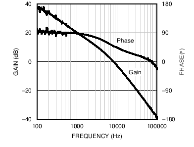
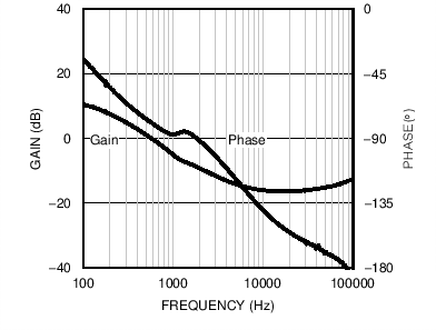
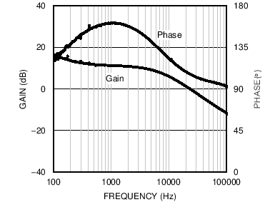
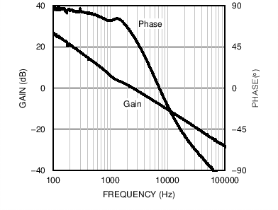
The plots shown in Figure 21 through Figure 26 show the gain and phase diagrams of the design example. The overall bandwidth is lower in a buck-boost application due the compensation challenges associated with the right-half-plane zero. For a pure buck application, the bandwidth could be much higher. The LM5116 data sheet is a good reference for compensation design of a pure buck mode regulator.
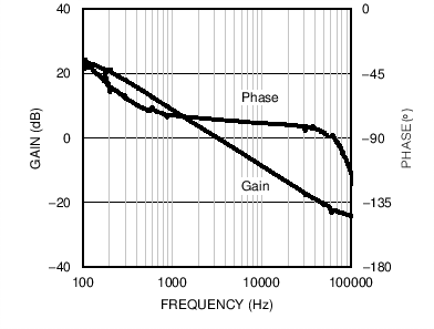
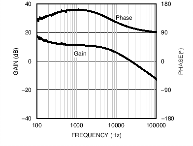
LM25118 21 Mod Buck.pngFigure 21. Modulator Gain and Phase - Buck Mode
LM25118 23 Error Amp Buck.pngFigure 23. Error Amplifier Gain and Phase - Buck Mode
LM25118 25 Overall Buck.pngFigure 25. Overall Loop Gain and Phase - Buck Mode
LM25118 22 Mod Buck Boost.pngFigure 22. Modulator Gain and Phase - Buck-Boost Mode
LM25118 24 Error Amp Buck Boost.pngFigure 24. Error Amplifier Gain and Phase - Buck-Boost Mode
LM25118 26 Overall Buck Boost.pngFigure 26. Overall Loop Gain and Phase - Buck-Boost Mode