SNVS726F July 2011 – March 2018 LM25118
PRODUCTION DATA.
- 1 Features
- 2 Applications
- 3 Description
- 4 Revision History
- 5 Pin Configuration and Functions
- 6 Specifications
- 7 Detailed Description
-
8 Application and Implementation
- 8.1 Application Information
- 8.2
Typical Application
- 8.2.1 Design Requirements
- 8.2.2
Detailed Design Procedure
- 8.2.2.1 Custom Design With WEBENCH® Tools
- 8.2.2.2 R7 = RT
- 8.2.2.3 Inductor Selection – L1
- 8.2.2.4 R13 = RSENSE
- 8.2.2.5 C15 = CRAMP
- 8.2.2.6 Inductor Current Limit Calculation
- 8.2.2.7 C9 - C12 = Output Capacitors
- 8.2.2.8 D1
- 8.2.2.9 D4
- 8.2.2.10 C1 – C5 = Input Capacitors
- 8.2.2.11 C20
- 8.2.2.12 C8
- 8.2.2.13 C16 = CSS
- 8.2.2.14 R8, R9
- 8.2.2.15 R1, R3, C21
- 8.2.2.16 R2
- 8.2.2.17 Snubber
- 8.2.2.18 Error Amplifier Configuration
- 8.2.3 Application Curves
- 9 Power Supply Recommendations
- 10Layout
- 11Device and Documentation Support
- 12Mechanical, Packaging, and Orderable Information
Package Options
Mechanical Data (Package|Pins)
- PWP|20
Thermal pad, mechanical data (Package|Pins)
- PWP|20
Orderable Information
7.3 Feature Description
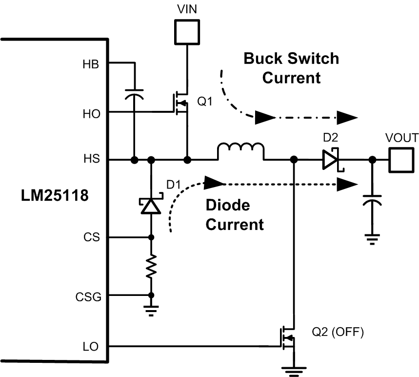
A buck-boost regulator can maintain regulation for input voltages either higher or lower than the output voltage. The challenge is that buck-boost power converters are not as efficient as buck regulators. The LM25118 has been designed as a dual-mode controller whereby the power converter acts as a buck regulator while the input voltage is above the output. As the input voltage approaches the output voltage, a gradual transition to the buck-boost mode occurs. The dual mode approach maintains regulation over a wide range of input voltages, while maintaining the optimal conversion efficiency in the normal buck mode. The gradual transition between modes eliminates disturbances at the output during transitions. Figure 8 shows the basic operation of the LM25118 regulator in the buck mode. In buck mode, transistor Q1 is active and Q2 is disabled. The inductor current ramps in proportion to the Vin – Vout voltage difference when Q1 is active and ramps down through the recirculating diode D1 when Q1 is off. The first order buck mode transfer function is VOUT/VIN = D, where D is the duty cycle of the buck switch, Q1.
 Figure 8. Buck Mode Operation
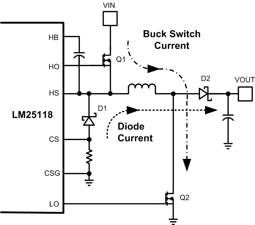
Figure 9 shows the basic operation of buck-boost mode. In buck-boost mode, both Q1 and Q2 are active for the same time interval each cycle. The inductor current ramps up (proportional to VIN) when Q1 and Q2 are active and ramps down through the recirculating diode during the off-time. The first order buck-boost transfer function is VOUT/VIN = D/(1 – D), where D is the duty cycle of Q1 and Q2.
 Figure 9. Buck-Boost Mode Operation
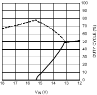
 Figure 10. Mode Dependence on Duty Cycle (VOUT =12 V)