SNVSBV5B December 2020 – December 2021 LM25149
PRODUCTION DATA
- 1 Features
- 2 Applications
- 3 Description
- 4 Revision History
- 5 Description (continued)
- 6 Pin Configuration and Functions
- 7 Specifications
-
8 Detailed Description
- 8.1 Overview
- 8.2 Functional Block Diagram
- 8.3
Feature Description
- 8.3.1 Input Voltage Range (VIN)
- 8.3.2 High-Voltage Bias Supply Regulator (VCC, VCCX, VDDA)
- 8.3.3 Precision Enable (EN)
- 8.3.4 Power-Good Monitor (PG)
- 8.3.5 Switching Frequency (RT)
- 8.3.6 Active EMI Filter
- 8.3.7 Dual Random Spread Spectrum (DRSS)
- 8.3.8 Soft Start
- 8.3.9 Output Voltage Setpoint (FB)
- 8.3.10 Minimum Controllable On Time
- 8.3.11 Error Amplifier and PWM Comparator (FB, EXTCOMP)
- 8.3.12 Slope Compensation
- 8.3.13 Inductor Current Sense (ISNS+, VOUT)
- 8.3.14 Hiccup Mode Current Limiting
- 8.3.15 High-Side and Low-Side Gate Drivers (HO, LO)
- 8.3.16 Output Configurations (CNFG)
- 8.3.17 Single-Output Dual-Phase Operation
- 8.4 Device Functional Modes
-
9 Application and Implementation
- 9.1 Application Information
- 9.2
Typical Applications
- 9.2.1
Design 1 – High Efficiency 2.1-MHz Synchronous
Buck Regulator
- 9.2.1.1 Design Requirements
- 9.2.1.2
Detailed Design Procedure
- 9.2.1.2.1 Custom Design With WEBENCH® Tools
- 9.2.1.2.2 Custom Design With Excel Quickstart Tool
- 9.2.1.2.3 Buck Inductor
- 9.2.1.2.4 Current-Sense Resistance
- 9.2.1.2.5 Output Capacitors
- 9.2.1.2.6 Input Capacitors
- 9.2.1.2.7 Frequency Set Resistor
- 9.2.1.2.8 Feedback Resistors
- 9.2.1.2.9 Compensation Components
- 9.2.1.2.10 Active EMI Components
- 9.2.1.3 Application Curves
- 9.2.2 Design 2 – High Efficiency 440-kHz Synchronous Buck Regulator
- 9.2.3 Design 3 – Dual-Phase 400-kHz 20-A Synchronous Buck Regulator
- 9.2.1
Design 1 – High Efficiency 2.1-MHz Synchronous
Buck Regulator
- 10Power Supply Recommendations
- 11Layout
- 12Device and Documentation Support
- 13Mechanical, Packaging, and Orderable Information
Package Options
Mechanical Data (Package|Pins)
- RGY|24
Thermal pad, mechanical data (Package|Pins)
- RGY|24
Orderable Information
9.1.1.6 Active EMI Filter
Active EMI filtering uses a capacitive multiplier to reduce the magnitude of the LC filtering components. Extra compensation components are needed, but the reduction in LC size outweigh the required network. The active EMI filter design steps are as follows:
- Calculate the required attenuation of the EMI filter at the switching frequency, similar to the passive EMI filter.
- Select input filter inductor LIN between 0.47 µH and 4.7 µH, lower than the passive EMI inductor.
- Use recommended values for sensing and compensation components CSEN, CAEFC, RAEFC, CINC, and RINC.
- Calculate active EMI injection capacitor CINJ.
- Calculate active EMI damping resistor RDAMP.
- For low-frequency designs (FSW < 1 MHz), calculate the active EMI damping capacitance CDAMP.Figure 9-3 Active EMI Filter for a Buck Regulator
Use Equation 20 to determine the attenuation required. Table 9-2 lists the recommended compensation and sensing component values. Use low FSW component values if FSW ≤ 1 MHz and high FSW component values if FSW > 1MHz.
| AEF COMPONENT | LOW FSW | HIGH FSW | DESCRIPTION |
|---|---|---|---|
| CSEN | 0.1 µF | 0.1 µF | Sensing capacitor |
| RAEFC | 1 kΩ | 200 Ω | Compensation |
| CAEFC | 1 nF | 5 nF | Compensation |
| RINC | 0.47 Ω | 0.47 Ω | Compensation |
| CINC | 0.1 µF | 0.1 µF | Compensation |
| RAEFVDD | 3 Ω | 3 Ω | Decoupling |
| CAEFVDD | 2.2 µF | 2.2 µF | Decoupling |
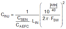
Select the desired LIN. Determine the Active EMI filter capacitance CINJ from Equation 25.
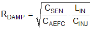
Determine the Active EMI damping resistor RDAMP from Equation 26.
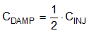
Determine the Active EMI damping capacitance CDAMP from Equation 27. CDAMP is not needed for FSW > 1 MHz.