SNVSBV5B December 2020 – December 2021 LM25149
PRODUCTION DATA
- 1 Features
- 2 Applications
- 3 Description
- 4 Revision History
- 5 Description (continued)
- 6 Pin Configuration and Functions
- 7 Specifications
-
8 Detailed Description
- 8.1 Overview
- 8.2 Functional Block Diagram
- 8.3
Feature Description
- 8.3.1 Input Voltage Range (VIN)
- 8.3.2 High-Voltage Bias Supply Regulator (VCC, VCCX, VDDA)
- 8.3.3 Precision Enable (EN)
- 8.3.4 Power-Good Monitor (PG)
- 8.3.5 Switching Frequency (RT)
- 8.3.6 Active EMI Filter
- 8.3.7 Dual Random Spread Spectrum (DRSS)
- 8.3.8 Soft Start
- 8.3.9 Output Voltage Setpoint (FB)
- 8.3.10 Minimum Controllable On Time
- 8.3.11 Error Amplifier and PWM Comparator (FB, EXTCOMP)
- 8.3.12 Slope Compensation
- 8.3.13 Inductor Current Sense (ISNS+, VOUT)
- 8.3.14 Hiccup Mode Current Limiting
- 8.3.15 High-Side and Low-Side Gate Drivers (HO, LO)
- 8.3.16 Output Configurations (CNFG)
- 8.3.17 Single-Output Dual-Phase Operation
- 8.4 Device Functional Modes
-
9 Application and Implementation
- 9.1 Application Information
- 9.2
Typical Applications
- 9.2.1
Design 1 – High Efficiency 2.1-MHz Synchronous
Buck Regulator
- 9.2.1.1 Design Requirements
- 9.2.1.2
Detailed Design Procedure
- 9.2.1.2.1 Custom Design With WEBENCH® Tools
- 9.2.1.2.2 Custom Design With Excel Quickstart Tool
- 9.2.1.2.3 Buck Inductor
- 9.2.1.2.4 Current-Sense Resistance
- 9.2.1.2.5 Output Capacitors
- 9.2.1.2.6 Input Capacitors
- 9.2.1.2.7 Frequency Set Resistor
- 9.2.1.2.8 Feedback Resistors
- 9.2.1.2.9 Compensation Components
- 9.2.1.2.10 Active EMI Components
- 9.2.1.3 Application Curves
- 9.2.2 Design 2 – High Efficiency 440-kHz Synchronous Buck Regulator
- 9.2.3 Design 3 – Dual-Phase 400-kHz 20-A Synchronous Buck Regulator
- 9.2.1
Design 1 – High Efficiency 2.1-MHz Synchronous
Buck Regulator
- 10Power Supply Recommendations
- 11Layout
- 12Device and Documentation Support
- 13Mechanical, Packaging, and Orderable Information
Package Options
Mechanical Data (Package|Pins)
- RGY|24
Thermal pad, mechanical data (Package|Pins)
- RGY|24
Orderable Information
9.1.1.4 Power MOSFETs
The choice of power MOSFETs has significant impact on DC/DC regulator performance. A MOSFET with low on-state resistance, RDS(on), reduces conduction loss, whereas low parasitic capacitances enable faster transition times and reduced switching loss. Normally, the lower the RDS(on) of a MOSFET, the higher the gate charge and output charge (QG and QOSS, respectively), and vice versa. As a result, the product of RDS(on) and QG is commonly specified as a MOSFET figure-of-merit. Low thermal resistance of a given package ensures that the MOSFET power dissipation does not result in excessive MOSFET die temperature.
The main parameters affecting power MOSFET selection in a LM25149 application are as follows:
- RDS(on) at VGS = 5 V
- Drain-source voltage rating, BVDSS, typically 40 V, 60 V, depending on the maximum input voltage
- Gate charge parameters at VGS = 5 V
- Output charge, QOSS, at the relevant input voltage
- Body diode reverse recovery charge, QRR
- Gate threshold voltage, VGS(th), derived from the Miller plateau evident in the QG versus VGS plot in the MOSFET data sheet. With a Miller plateau voltage typically in the range of 2 V to 3 V, the 5-V gate drive amplitude of the LM25149 provides an adequately enhanced MOSFET when on and a margin against Cdv/dt shootthrough when off.
The MOSFET-related power losses for one channel are summarized by the equations presented in Table 9-1, where suffixes one and two represent high-side and low-side MOSFET parameters, respectively. While the influence of inductor ripple current is considered, second-order loss modes, such as those related to parasitic inductances and SW node ringing, are not included. Consult the LM25149 Quickstart Calculator.
| POWER LOSS MODE | HIGH-SIDE MOSFET | LOW-SIDE MOSFET |
|---|---|---|
| MOSFET conduction(2)(3) | 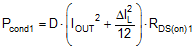 | 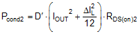 |
| MOSFET switching | 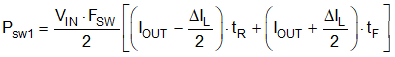 | Negligible |
| MOSFET gate drive(1) | 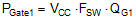 | 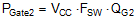 |
| MOSFET output charge(4) |  | |
| Body diode conduction | N/A | 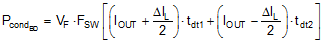 |
| Body diode reverse recovery(5) |  | |
The high-side (control) MOSFET carries the inductor current during the PWM on time (or D interval) and typically incurs most of the switching losses. It is, therefore, imperative to choose a high-side MOSFET that balances conduction and switching loss contributions. The total power dissipation in the high-side MOSFET is the sum of the losses due to conduction, switching (voltage-current overlap), output charge, and typically two-thirds of the net loss attributed to body diode reverse recovery.
The low-side (synchronous) MOSFET carries the inductor current when the high-side MOSFET is off (or during the 1–D interval). The low-side MOSFET switching loss is negligible as it is switched at zero voltage – current just commutates from the channel to the body diode or vice versa during the transition deadtimes. LM25149, with its adaptive gate drive timing, minimizes body diode conduction losses when both MOSFETs are off. Such losses scale directly with switching frequency.
In high step-down ratio applications, the low-side MOSFET carries the current for a large portion of the switching period. Therefore, to attain high efficiency, it is critical to optimize the low-side MOSFET for low RDS(on). In cases where the conduction loss is too high or the target RDS(on) is lower than available in a single MOSFET, connect two low-side MOSFETs in parallel. The total power dissipation of the low-side MOSFET is the sum of the losses due to channel conduction, body diode conduction, and typically one-third of the net loss attributed to body diode reverse recovery. The LM25149 is well suited to drive TI's portfolio of NexFET™ power MOSFETs.