SNVSBL7A March 2020 – August 2020 LM25184
PRODUCTION DATA
- 1 Features
- 2 Applications
- 3 Description
- 4 Revision History
- 5 Pin Configuration and Functions
- 6 Specifications
-
7 Detailed Description
- 7.1 Overview
- 7.2 Functional Block Diagram
- 7.3
Feature Description
- 7.3.1 Integrated Power MOSFET
- 7.3.2 PSR Flyback Modes of Operation
- 7.3.3 Setting the Output Voltage
- 7.3.4 Control Loop Error Amplifier
- 7.3.5 Precision Enable
- 7.3.6 Configurable Soft Start
- 7.3.7 External Bias Supply
- 7.3.8 Minimum On-Time and Off-Time
- 7.3.9 Overcurrent Protection
- 7.3.10 Thermal Shutdown
- 7.4 Device Functional Modes
-
8 Application and Implementation
- 8.1 Application Information
- 8.2
Typical Applications
- 8.2.1
Design 1: Wide VIN, Low IQ PSR Flyback Converter Rated at 12 V, 1 A
- 8.2.1.1 Design Requirements
- 8.2.1.2
Detailed Design Procedure
- 8.2.1.2.1 Custom Design With WEBENCH® Tools
- 8.2.1.2.2 Custom Design With Excel Quickstart Tool
- 8.2.1.2.3 Flyback Transformer – T1
- 8.2.1.2.4 Flyback Diode – DFLY
- 8.2.1.2.5 Leakgae Inductance Clamp Circuit – DF, DCLAMP
- 8.2.1.2.6 Output Capacitor – COUT
- 8.2.1.2.7 Input Capacitor – CIN
- 8.2.1.2.8 Feedback Resistor – RFB
- 8.2.1.2.9 Thermal Compensation Resistor – RTC
- 8.2.1.2.10 UVLO Resistors – RUV1, RUV2
- 8.2.1.2.11 Soft-Start Capacitor – CSS
- 8.2.2 Application Curves
- 8.2.3 Design 2: PSR Flyback Converter With Dual Outputs of 15 V and –8 V at 0.5 A
- 8.2.1
Design 1: Wide VIN, Low IQ PSR Flyback Converter Rated at 12 V, 1 A
- 9 Power Supply Recommendations
- 10Layout
- 11Device and Documentation Support
- 12Mechanical, Packaging, and Orderable Information
Package Options
Mechanical Data (Package|Pins)
- NGU|8
Thermal pad, mechanical data (Package|Pins)
Orderable Information
8.2.1.2.6 Output Capacitor – COUT
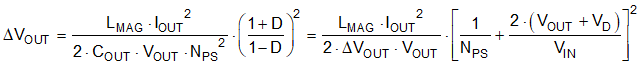
The output capacitor determines the voltage ripple at the converter output, limits the voltage excursion during a load transient, and sets the dominant pole of the small-signal response of the converter. Select an output capacitance using Equation 22 to limit the ripple voltage amplitude to less than 1% of the output voltage at minimum input voltage and maximum load.
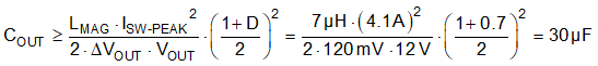
Mindful of the voltage coefficient of ceramic capacitors, select four 22-µF, 25-V capacitors in 1210 case size with X7S or better dielectric. Assuming operation in BCM, calculate the capacitive ripple voltage at the output using Equation 23.
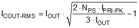
Equation 24 gives an expression for the output capacitor RMS ripple current.