SNVSBL7A March 2020 – August 2020 LM25184
PRODUCTION DATA
- 1 Features
- 2 Applications
- 3 Description
- 4 Revision History
- 5 Pin Configuration and Functions
- 6 Specifications
-
7 Detailed Description
- 7.1 Overview
- 7.2 Functional Block Diagram
- 7.3
Feature Description
- 7.3.1 Integrated Power MOSFET
- 7.3.2 PSR Flyback Modes of Operation
- 7.3.3 Setting the Output Voltage
- 7.3.4 Control Loop Error Amplifier
- 7.3.5 Precision Enable
- 7.3.6 Configurable Soft Start
- 7.3.7 External Bias Supply
- 7.3.8 Minimum On-Time and Off-Time
- 7.3.9 Overcurrent Protection
- 7.3.10 Thermal Shutdown
- 7.4 Device Functional Modes
-
8 Application and Implementation
- 8.1 Application Information
- 8.2
Typical Applications
- 8.2.1
Design 1: Wide VIN, Low IQ PSR Flyback Converter Rated at 12 V, 1 A
- 8.2.1.1 Design Requirements
- 8.2.1.2
Detailed Design Procedure
- 8.2.1.2.1 Custom Design With WEBENCH® Tools
- 8.2.1.2.2 Custom Design With Excel Quickstart Tool
- 8.2.1.2.3 Flyback Transformer – T1
- 8.2.1.2.4 Flyback Diode – DFLY
- 8.2.1.2.5 Leakgae Inductance Clamp Circuit – DF, DCLAMP
- 8.2.1.2.6 Output Capacitor – COUT
- 8.2.1.2.7 Input Capacitor – CIN
- 8.2.1.2.8 Feedback Resistor – RFB
- 8.2.1.2.9 Thermal Compensation Resistor – RTC
- 8.2.1.2.10 UVLO Resistors – RUV1, RUV2
- 8.2.1.2.11 Soft-Start Capacitor – CSS
- 8.2.2 Application Curves
- 8.2.3 Design 2: PSR Flyback Converter With Dual Outputs of 15 V and –8 V at 0.5 A
- 8.2.1
Design 1: Wide VIN, Low IQ PSR Flyback Converter Rated at 12 V, 1 A
- 9 Power Supply Recommendations
- 10Layout
- 11Device and Documentation Support
- 12Mechanical, Packaging, and Orderable Information
Package Options
Mechanical Data (Package|Pins)
- NGU|8
Thermal pad, mechanical data (Package|Pins)
Orderable Information
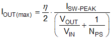
7.3.9 Overcurrent Protection
In case of an overcurrent condition on the isolated output or outputs, the output voltage drops lower than the regulation level since the maximum power delivered is limited by the peak current capability on the primary side. The peak primary current is maintained at 2.5 A (plus an amount related to the 100-ns propagation delay of the current limit comparator) until the output decreases to the secondary diode voltage drop to impact the reflected signal on the primary side. At this point, the LM25184 assumes the output cannot be recovered and re-calibrates its switching frequency to 9 kHz until the overload condition is removed. The LM25184 responds with similar behavior to an output short circuit condition.
For a given input voltage, Equation 13 gives the maximum output current prior to the engagement of overcurrent protection. The typical threshold value for ISW-PEAK from Section 6.5 is 4.1 A.