SNVSBL7A March 2020 – August 2020 LM25184
PRODUCTION DATA
- 1 Features
- 2 Applications
- 3 Description
- 4 Revision History
- 5 Pin Configuration and Functions
- 6 Specifications
-
7 Detailed Description
- 7.1 Overview
- 7.2 Functional Block Diagram
- 7.3
Feature Description
- 7.3.1 Integrated Power MOSFET
- 7.3.2 PSR Flyback Modes of Operation
- 7.3.3 Setting the Output Voltage
- 7.3.4 Control Loop Error Amplifier
- 7.3.5 Precision Enable
- 7.3.6 Configurable Soft Start
- 7.3.7 External Bias Supply
- 7.3.8 Minimum On-Time and Off-Time
- 7.3.9 Overcurrent Protection
- 7.3.10 Thermal Shutdown
- 7.4 Device Functional Modes
-
8 Application and Implementation
- 8.1 Application Information
- 8.2
Typical Applications
- 8.2.1
Design 1: Wide VIN, Low IQ PSR Flyback Converter Rated at 12 V, 1 A
- 8.2.1.1 Design Requirements
- 8.2.1.2
Detailed Design Procedure
- 8.2.1.2.1 Custom Design With WEBENCH® Tools
- 8.2.1.2.2 Custom Design With Excel Quickstart Tool
- 8.2.1.2.3 Flyback Transformer – T1
- 8.2.1.2.4 Flyback Diode – DFLY
- 8.2.1.2.5 Leakgae Inductance Clamp Circuit – DF, DCLAMP
- 8.2.1.2.6 Output Capacitor – COUT
- 8.2.1.2.7 Input Capacitor – CIN
- 8.2.1.2.8 Feedback Resistor – RFB
- 8.2.1.2.9 Thermal Compensation Resistor – RTC
- 8.2.1.2.10 UVLO Resistors – RUV1, RUV2
- 8.2.1.2.11 Soft-Start Capacitor – CSS
- 8.2.2 Application Curves
- 8.2.3 Design 2: PSR Flyback Converter With Dual Outputs of 15 V and –8 V at 0.5 A
- 8.2.1
Design 1: Wide VIN, Low IQ PSR Flyback Converter Rated at 12 V, 1 A
- 9 Power Supply Recommendations
- 10Layout
- 11Device and Documentation Support
- 12Mechanical, Packaging, and Orderable Information
Package Options
Mechanical Data (Package|Pins)
- NGU|8
Thermal pad, mechanical data (Package|Pins)
Orderable Information
3 Description
The LM25184 is a primary-side regulated (PSR) flyback converter with high efficiency over a wide input voltage range of 4.5 V to 42 V. The isolated output voltage is sampled from the primary-side flyback voltage. The high level of integration results in a simple, reliable, and high-density design with only one component crossing the isolation barrier. Boundary conduction mode (BCM) switching enables a compact magnetic solution and better than ±1.5% load and line regulation performance. An integrated 65-V power MOSFET provides output power up to 15 W with enhanced headroom for line transients.
The LM25184 simplifies the implementation of isolated DC/DC supplies with optional features to optimize performance for the target end equipment. The output voltage is set by one resistor, while an optional resistor improves output voltage accuracy by negating the thermal coefficient of the flyback diode voltage drop. Additional features include an internally-fixed or externally-programmable soft-start, precision enable input with hysteresis for adjustable line UVLO, hiccup-mode overload protection, and thermal shutdown protection with automatic recovery.
The LM25184 flyback converter is available in a 8-pin, 4-mm × 4-mm, thermally-enhanced WSON package with 0.8-mm pin pitch.
| PART NUMBER (1) | PACKAGE | BODY SIZE (NOM) |
|---|---|---|
| LM25184 | WSON (8) | 4.00 mm × 4.00 mm |
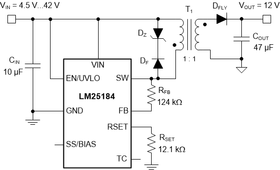
 Typical Application
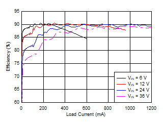
 Typical Efficiency, VOUT = 12 V