SNVS116E May 1998 – December 2014 LM3420
PRODUCTION DATA.
- 1 Features
- 2 Applications
- 3 Description
- 4 Revision History
- 5 Pin Configuration and Functions
- 6 Specifications
- 7 Parameter Measurement Information
- 8 Detailed Description
-
9 Application and Implementation
- 9.1 Application Information
- 9.2
Typical Application: Constant Current/Constant Voltage Li-Ion Battery Charger
- 9.2.1 Design Requirements
- 9.2.2 Detailed Design Procedure
- 9.2.3 Application Curve
- 9.2.4
Other Application Circuits
- 9.2.4.1 Low Dropout Constant Current/Constant Voltage 2-Cell Charger
- 9.2.4.2 High-Efficiency Switching Regulator Constant Current/Constant Voltage 2-Cell Charger
- 9.2.4.3 Low Dropout Constant Current/Constant Voltage Li-Ion Battery Charger
- 9.2.4.4 High-Efficiency Switching Charger With High Side Current Sensing
- 9.2.4.5 Fast-Pulsed Constant Current 2-Cell Charger
- 9.2.4.6 MOSFET Low Dropout Charger
- 10Power Supply Recommendations
- 11Layout
- 12Device and Documentation Support
- 13Mechanical, Packaging, and Orderable Information
Package Options
Mechanical Data (Package|Pins)
- DBV|5
Thermal pad, mechanical data (Package|Pins)
Orderable Information
8 Detailed Description
8.1 Overview
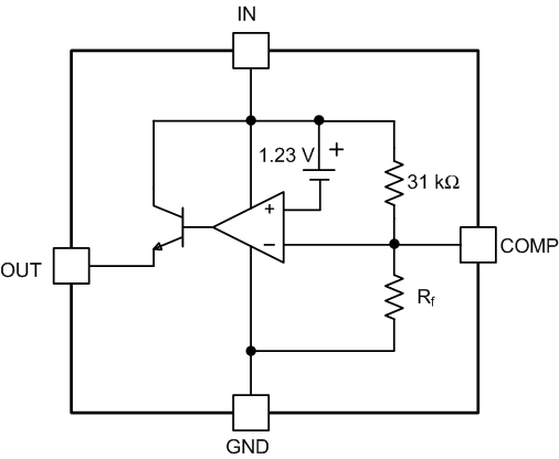
The LM3420 is a shunt regulator specifically designed to be the reference and control section in an overall feedback loop of a lithium-ion battery charger. The regulated output voltage is sensed between the IN pin and GROUND pin of the LM3420. If the voltage at the IN pin is less than the LM3420 regulating voltage (VREG), the OUT pin sources no current. As the voltage at the IN pin approaches the VREG voltage, the OUT pin begins sourcing current. This current is then used to drive a feedback device (opto-coupler), or a power device (linear regulator, switching regulator, etc.), which servos the output voltage to be the same value as VREG.
In some applications, (even under normal operating conditions) the voltage on the IN pin can be forced above the VREG voltage. In these instances, the maximum voltage applied to the IN pin should not exceed 20 V. In addition, an external resistor may be required on the OUT pin to limit the maximum current to 20 mA.
8.2 Functional Block Diagram
8.3 Feature Description
8.3.1 Compensation
The inverting input of the error amplifier is brought out to allow overall closed-loop compensation. In many of the applications circuits shown here, compensation is provided by a single capacitor (CC) connected from the compensation pin to the out pin of the LM3420. The capacitor values shown in the schematics are adequate under most conditions, but they can be increased or decreased depending on the desired loop response. Applying a load pulse to the output of a regulator circuit and observing the resultant output voltage response is an easy method of determining the stability of the control loop.
Analyzing more complex feedback loops requires additional information.
The formula for AC gain at a frequency (f) is shown in Equation 1:
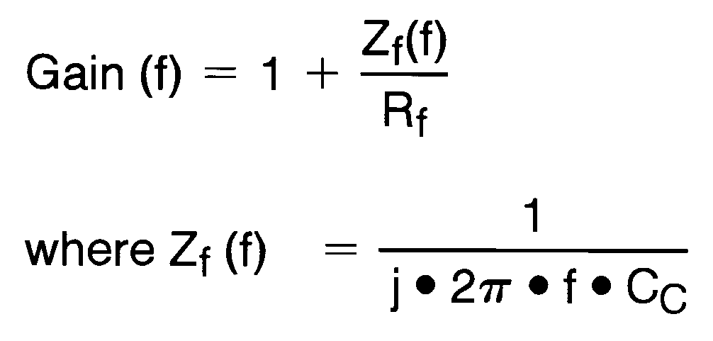
where
- Rf ≈ 181 kΩ
The resistor (Rf) in the formula is an internal resistor located on the die. Since this resistor value affects the phase margin, the worst case maximum and minimum values are important when analyzing closed loop stability. The minimum and maximum room temperature values of this resistor are specified in the LM3420 Electrical Characteristics section of this data sheet, and a curve showing the temperature coefficient is shown in the curves section. Minimum values of Rf result in lower phase margins.
8.3.2 VREG External Voltage Trim
The regulation voltage (VREG) of the LM3420 can be externally trimmed by adding a single resistor from the COMP pin to the +IN pin or from the COMP pin to the GND pin, depending on the desired trim direction. Trim adjustments up to ±10% of VREG can be realized, with only a small increase in the temperature coefficient. (See temperature coefficient curve shown in Figure 11.)
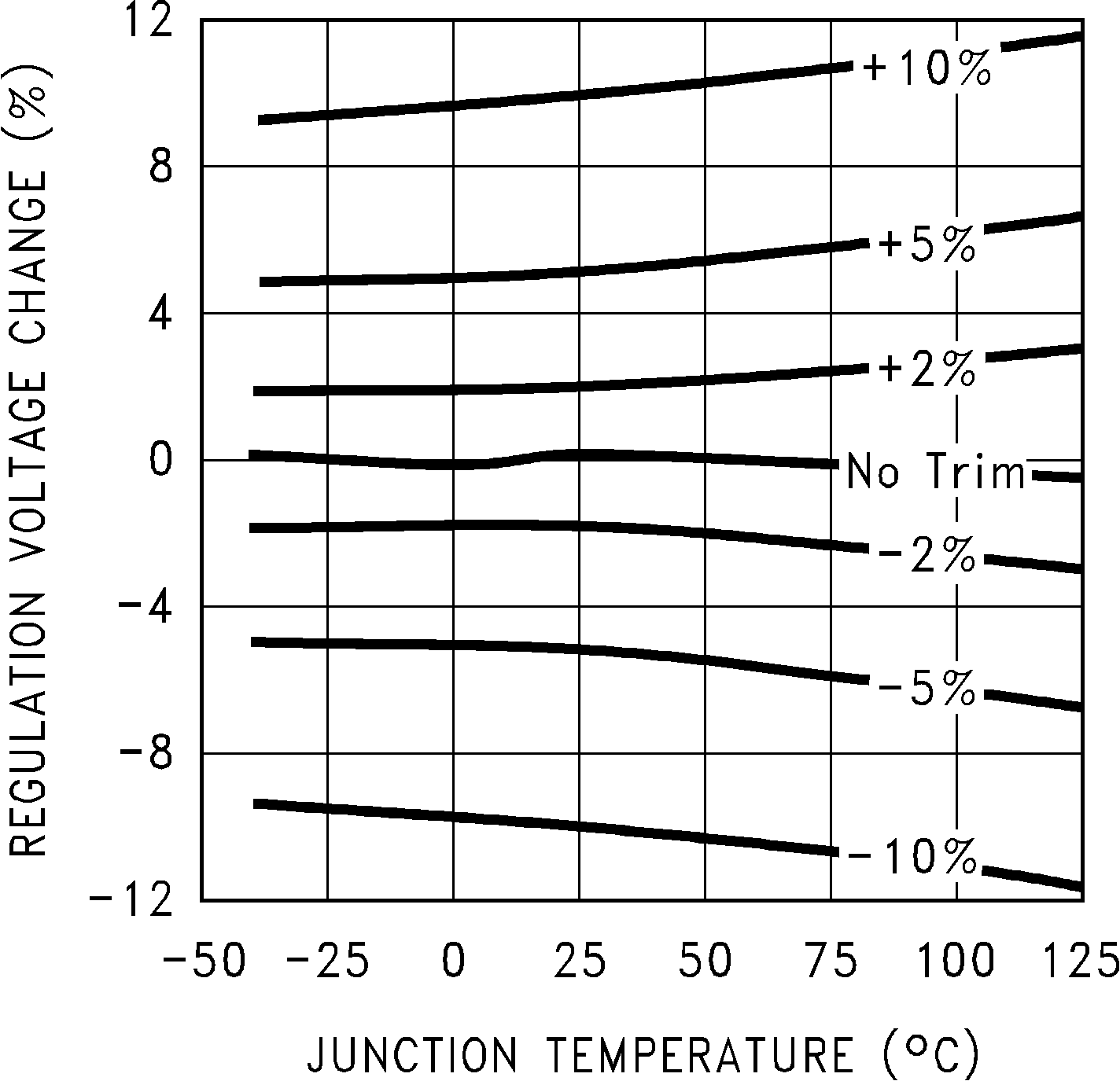 Figure 11. Normalized Temperature Drift With Output Externally Trimmed
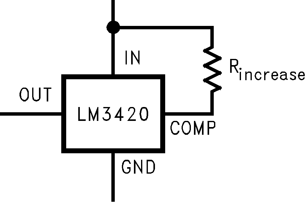
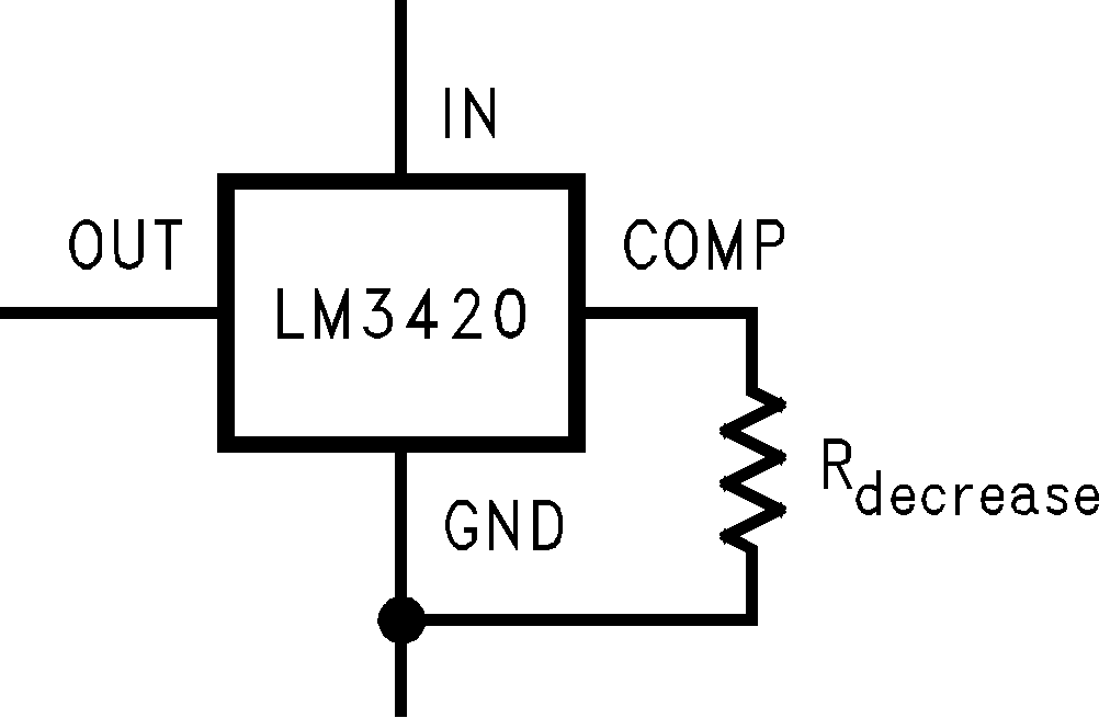
Formula for selecting trim resistor values is shown in Equation 2 and Equation 3, based on the percent of increase (%incr) or percent of decrease (%decr) of the output voltage from the nominal voltage.
8.4 Device Functional Modes
8.4.1 Operation as Control Section
The LM3420 is monolithic integrated circuits, which is suitable for charging and end-of-charge control for Lithium-Ion rechargeable batteries. In this application, LM3420 is the reference and control section in the overall feedback loop. The regulated voltage is sensed between the IN pin and GND pin. If the voltage at the IN pin is less than the regulating voltage (VREG), the OUT pin sources no current. As the voltage at the IN pin approaches the VREG, the OUT pin begins sourcing current, which can drive a feedback device or a power device.