SNVS116E May 1998 – December 2014 LM3420
PRODUCTION DATA.
- 1 Features
- 2 Applications
- 3 Description
- 4 Revision History
- 5 Pin Configuration and Functions
- 6 Specifications
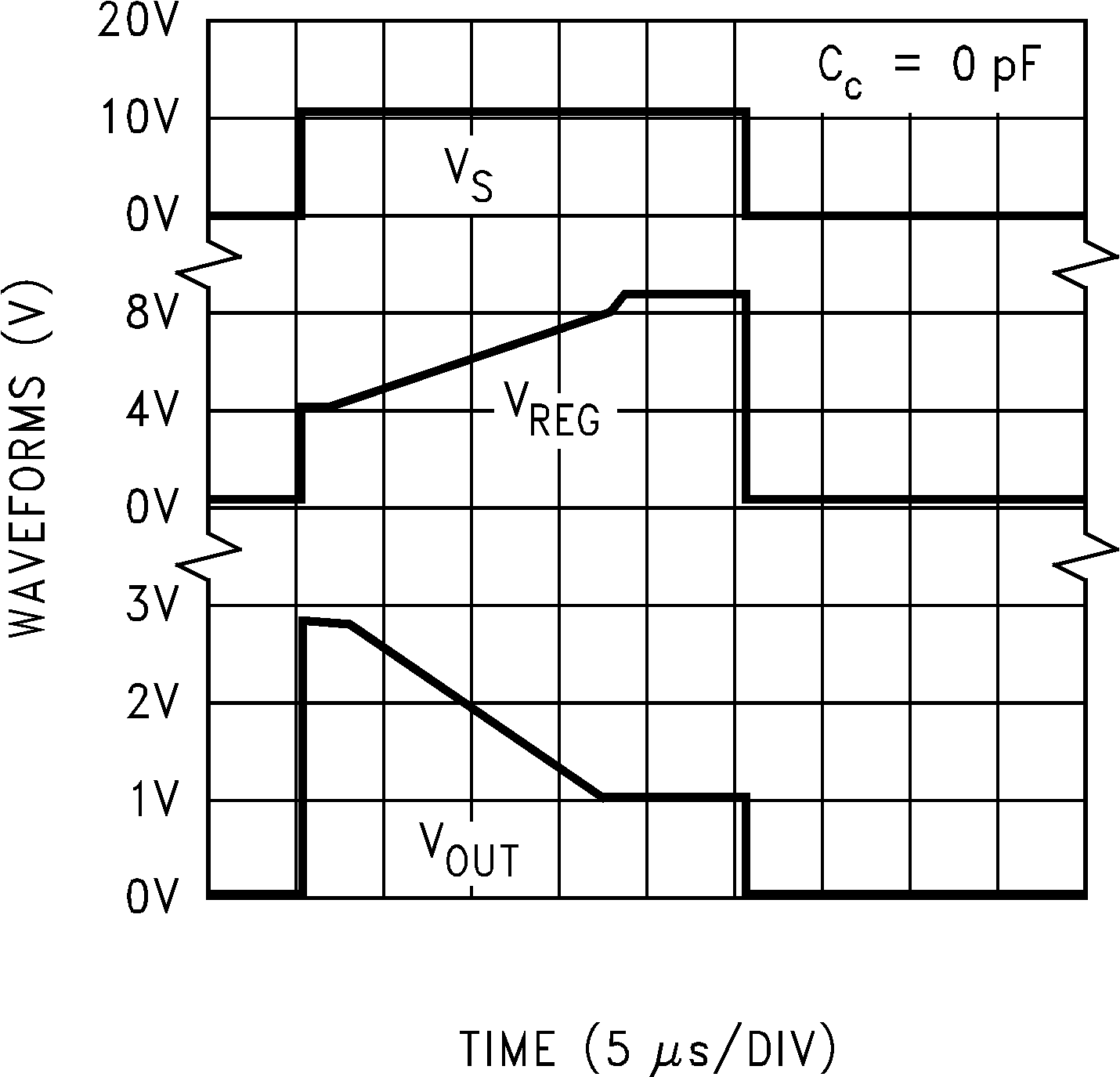
- 7 Parameter Measurement Information
- 8 Detailed Description
-
9 Application and Implementation
- 9.1 Application Information
- 9.2
Typical Application: Constant Current/Constant Voltage Li-Ion Battery Charger
- 9.2.1 Design Requirements
- 9.2.2 Detailed Design Procedure
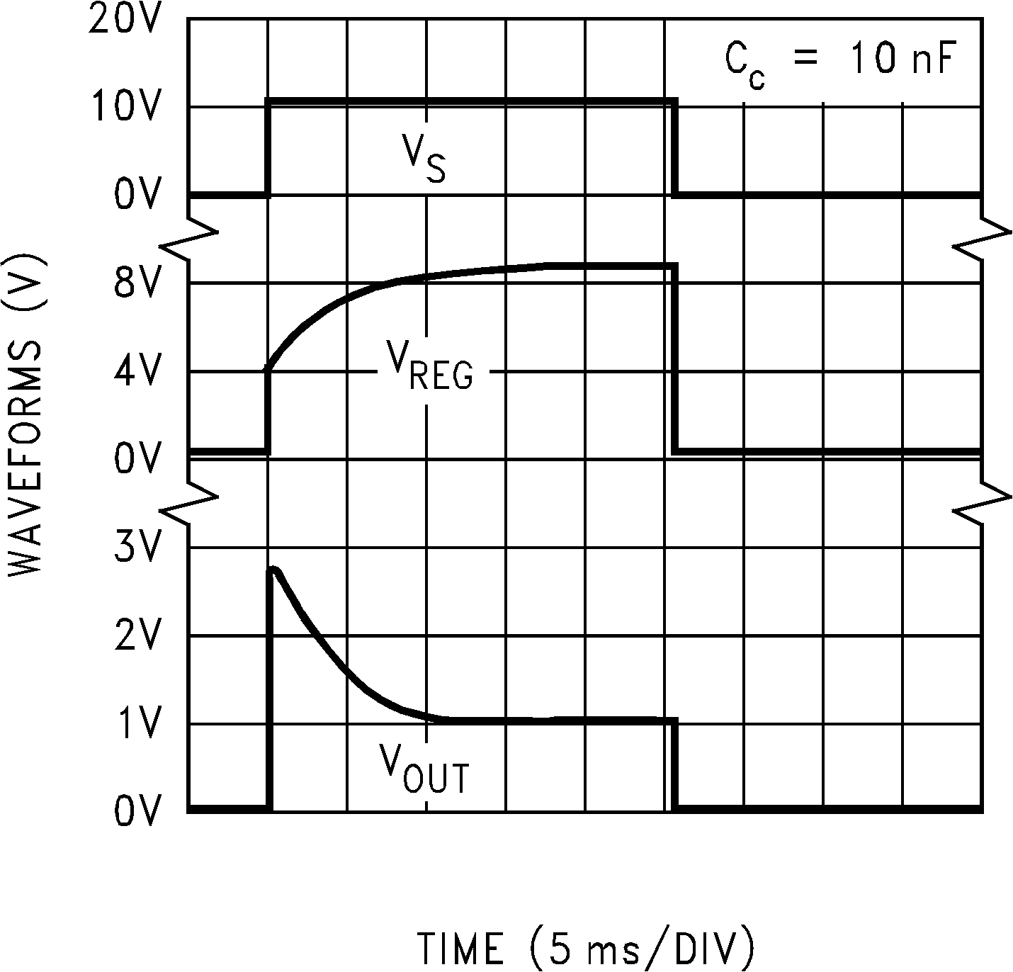
- 9.2.3 Application Curve
- 9.2.4
Other Application Circuits
- 9.2.4.1 Low Dropout Constant Current/Constant Voltage 2-Cell Charger
- 9.2.4.2 High-Efficiency Switching Regulator Constant Current/Constant Voltage 2-Cell Charger
- 9.2.4.3 Low Dropout Constant Current/Constant Voltage Li-Ion Battery Charger
- 9.2.4.4 High-Efficiency Switching Charger With High Side Current Sensing
- 9.2.4.5 Fast-Pulsed Constant Current 2-Cell Charger
- 9.2.4.6 MOSFET Low Dropout Charger
- 10Power Supply Recommendations
- 11Layout
- 12Device and Documentation Support
- 13Mechanical, Packaging, and Orderable Information
Package Options
Mechanical Data (Package|Pins)
- DBV|5
Thermal pad, mechanical data (Package|Pins)
Orderable Information
6 Specifications
6.1 Absolute Maximum Ratings
over operating free-air temperature range (unless otherwise noted) (1)(2)| MIN | MAX | UNIT | ||
|---|---|---|---|---|
| Input voltage VIN | 20 | V | ||
| Output current | 20 | mA | ||
| Junction temperature | 150 | °C | ||
| Lead temperature | Vapor phase (60 seconds) | 215 | ||
| Infrared (15 seconds) | 220 | |||
| Power dissipation (TA = 25°C)(3) | 300 | mV | ||
| Storage temperature, Tstg | −65 | 150 | °C | |
(1) Stresses beyond those listed under Absolute Maximum Ratings may cause permanent damage to the device. These are stress ratings only, which do not imply functional operation of the device at these or any other conditions beyond those indicated under Recommended Operating Conditions. Exposure to absolute-maximum-rated conditions for extended periods may affect device reliability.
(2) If Military/Aerospace specified devices are required, please contact the Texas Instruments Sales Office/Distributors for availability and specifications.
(3) The maximum power dissipation must be derated at elevated temperatures and is dictated by TJmax (maximum junction temperature), RθJA (junction-to-ambient thermal resistance), and TA (ambient temperature). The maximum allowable power dissipation at any temperature is PDmax = (TJmax − TA)/RθJA or the number given in the Absolute Maximum Ratings, whichever is lower. The typical thermal resistance (RθJA) when soldered to a printed circuit board is approximately 181.2°C/W for the DBV0005A package.
6.2 ESD Ratings
| VALUE | UNIT | |||
|---|---|---|---|---|
| V(ESD) | Electrostatic discharge | Human-body model (HBM), per ANSI/ESDA/JEDEC JS-001(1) | ±2000 | V |
| Charged-device model (CDM), per JEDEC specification JESD22-C101(2) | ±500 | |||
(1) JEDEC document JEP155 states that 500-V HBM allows safe manufacturing with a standard ESD control process.
(2) JEDEC document JEP157 states that 250-V CDM allows safe manufacturing with a standard ESD control process.
6.3 Recommended Operating Conditions
over operating free-air temperature range (unless otherwise noted)(1)(2)| MIN | NOM | MAX | UNIT | ||
|---|---|---|---|---|---|
| Ambient temperature | −40 | 85 | °C | ||
| Junction temperature | −40 | 125 | |||
| Output current | 15 | mA | |||
(1) Stresses beyond those listed under Absolute Maximum Ratings may cause permanent damage to the device. These are stress ratings only, which do not imply functional operation of the device at these or any other conditions beyond those indicated under Recommended Operating Conditions. Exposure to absolute-maximum-rated conditions for extended periods may affect device reliability.
(2) The maximum power dissipation must be derated at elevated temperatures and is dictated by TJmax (maximum junction temperature), RθJA (junction to ambient thermal resistance), and TA (ambient temperature). The maximum allowable power dissipation at any temperature is PDmax = (TJmax − TA)/RθJA or the number given in the Absolute Maximum Ratings, whichever is lower. The typical thermal resistance (RθJA) when soldered to a printed circuit board is approximately 181.2°C/W for the DBV0005A package.
6.4 Thermal Information
| THERMAL METRIC(1) | LM3420 | UNIT | |
|---|---|---|---|
| SOT-23 (DBV) | |||
| 5 PINS | |||
| RθJA | Junction-to-ambient thermal resistance | 181.2 | °C/W |
| RθJC(top) | Junction-to-case (top) thermal resistance | 91.2 | |
| RθJB | Junction-to-board thermal resistance | 38.2 | |
| ψJT | Junction-to-top characterization parameter | 5.3 | |
| ψJB | Junction-to-board characterization parameter | 37.7 | |
(1) For more information about traditional and new thermal metrics, see the IC Package Thermal Metrics application report, SPRA953.
6.5 LM3420 Electrical Characteristics
Unless otherwise specified, specifications apply over full operating temperature range and VIN = VREG, VOUT = 1.5 V.| PARAMETER | TEST CONDITIONS | MIN(2) | TYP(1) | MAX(2) | UNIT | |
|---|---|---|---|---|---|---|
| VREG | Regulation voltage | IOUT = 1 mA, TJ = 25°C | 8.316 | 8.4 | 8.484 | V |
| IOUT = 1 mA | 8.232 | 8.4 | 8.568 | |||
| Regulation voltage tolerance | IOUT = 1 mA, TJ = 25°C | –1% | 1% | |||
| IOUT = 1 mA | –2% | 2% | ||||
| IQ | Quiescent current | IOUT = 1 mA, TJ = 25°C | 85 | 125 | μA | |
| IOUT = 1 mA | 85 | 150 | ||||
| Gm | Transconductance ΔIOUT/ΔVREG |
20 μA ≤ IOUT ≤ 1 mA, VOUT = 6 V TJ = 25°C |
1 | 3.3 | mA/mV | |
| 20 μA ≤ IOUT ≤ 1 mA, VOUT = 6 V | 0.50 | 3.3 | ||||
| 1 mA ≤ IOUT ≤ 15 mA, VOUT = 6 V | 2.5 | 6 | ||||
| 1 mA ≤ IOUT ≤ 15 mA, VOUT = 6 V | 1.4 | 6 | ||||
| AV | Voltage gain ΔVOUT/ΔVREG |
1 V ≤ VOUT ≤ VREG − 1.2V, RL = 470 Ω(3)
TJ = 25°C |
450 | 1000 | V/V | |
| 1 V ≤ VOUT ≤ VREG − 1.3 V, RL = 470 Ω | 200 | 1000 | ||||
| 1 V ≤ VOUT ≤ VREG − 1.2 V, RL = 5 kΩ(3)
TJ = 25°C |
1000 | 3500 | V/V | |||
| 1 V ≤ VOUT ≤ VREG − 1.3 V, RL = 5 kΩ | 700 | 3500 | ||||
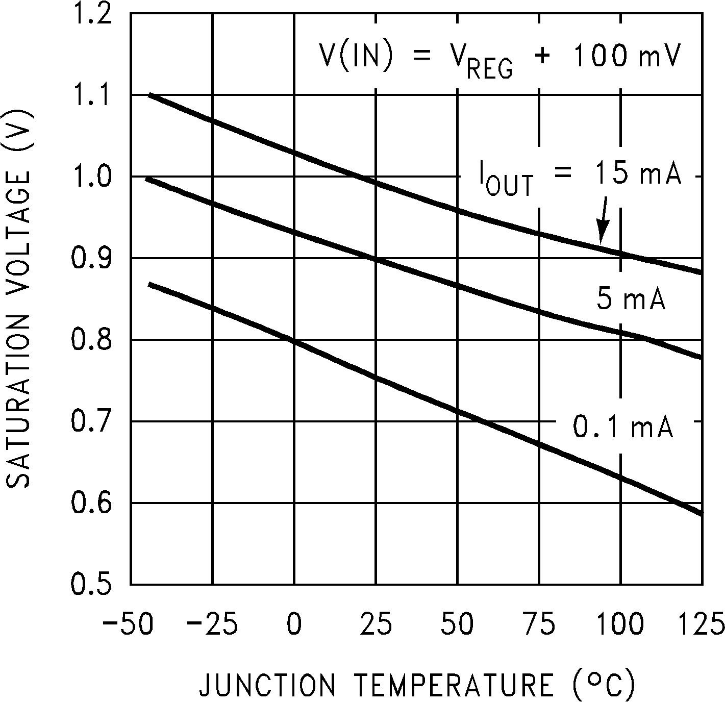
| VSAT | Output saturation(4) | VIN = VREG + 100 mV TJ = 25°C |
1 | 1.2 | V | |
| VIN = VREG + 100 mV | 1 | 1.3 | ||||
| IL | Output leakage current | VIN = VREG − 100 mV, VOUT = 0 V TJ = 25°C |
0.1 | 0.5 | μA | |
| VIN = VREG − 100 mV, VOUT = 0 V | 0.1 | 1 | ||||
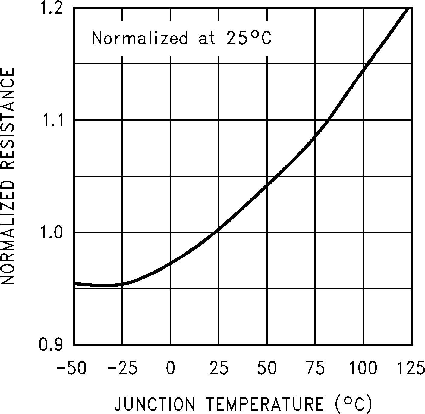
| Rf | Internal feedback resistor(5) | TJ = 25°C | 135 | 181 | 227 | kΩ |
| En | Output noise voltage | IOUT = 1 mA, 10 Hz ≤ f ≤ 10 kHz | 140 | μVRMS | ||
(1) Typical numbers are at 25°C and represent the most likely parametric norm.
(2) Limits are 100% production tested at 25°C. Limits over the operating temperature range are specified through correlation using Statistical Quality Control (SQC) methods. The limits are used to calculate Averaging Outgoing Quality Level (AOQL).
(3) Actual test is done using equivalent current sink instead of a resistor load.
(4) VSAT = V(IN) − VOUT, when the voltage at the IN pin is forced 100 mV above the nominal regulating voltage (VREG).
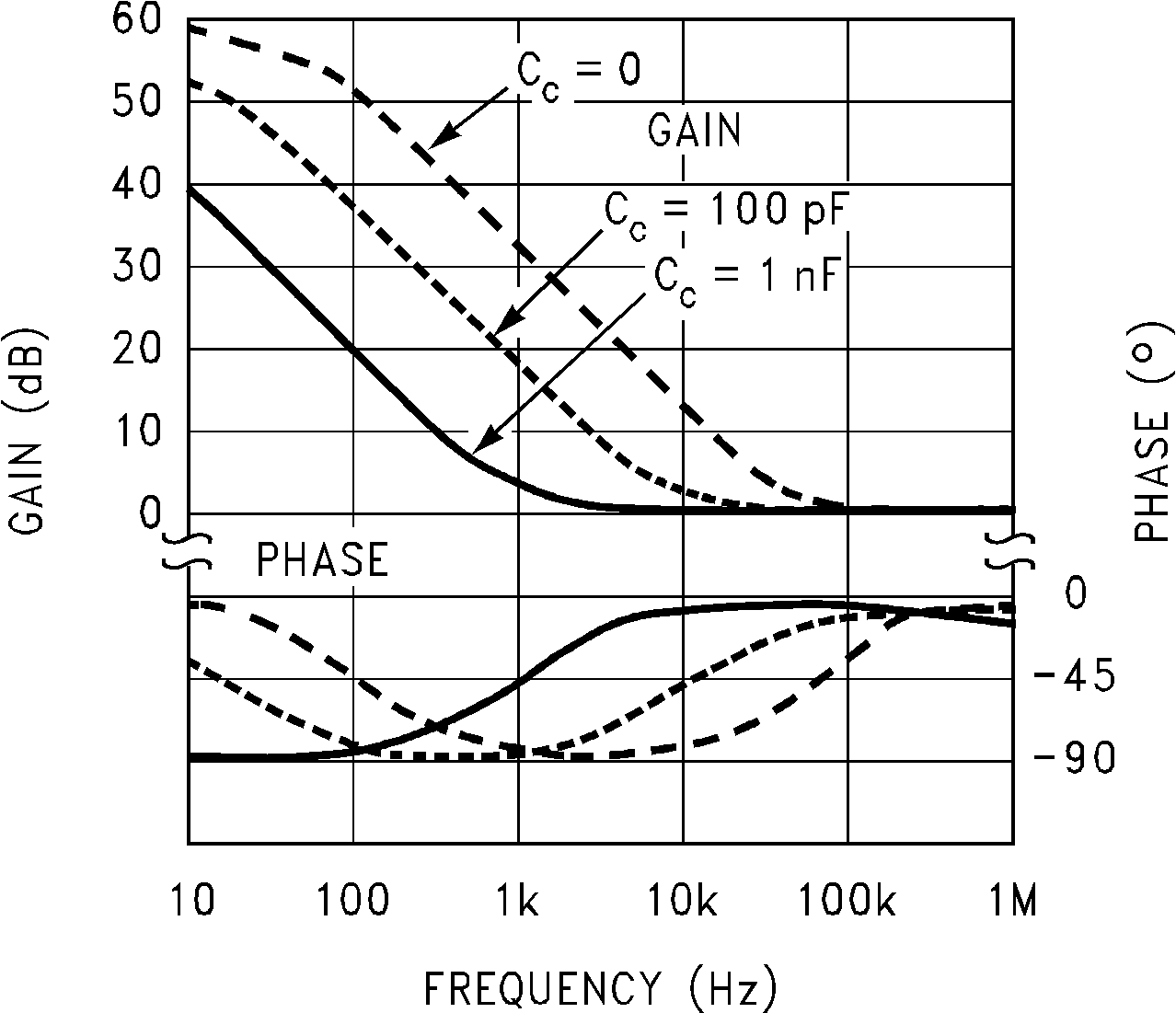
(5) See Application and Implementation and Typical Characteristics sections for information on this resistor.
6.6 LM3420A Electrical Characteristics
Unless otherwise specified, specifications apply over full operating temperature range and VIN = VREG, VOUT = 1.5 V.| PARAMETER | TEST CONDITIONS | MIN(2) | TYP(1) | MAX(2) | UNIT | |
|---|---|---|---|---|---|---|
| VREG | Regulation voltage | IOUT = 1 mA, TJ = 25°C | 8.358 | 8.4 | 8.442 | V |
| IOUT = 1 mA | 8.316 | 8.4 | 8.484 | |||
| Regulation voltage tolerance | IOUT = 1 mA, TJ = 25°C | –0.5% | 0.5% | |||
| IOUT = 1 mA | –1% | 1% | ||||
| IQ | Quiescent current | IOUT = 1 mA, TJ = 25°C | 85 | 110 | μA | |
| IOUT = 1 mA | 85 | 115 | ||||
| Gm | Transconductance ΔIOUT/ΔVREG |
20 μA ≤ IOUT ≤ 1 mA, VOUT = 6 V TJ = 25°C |
1.3 | 3.3 | mA/mV | |
| 20 μA ≤ IOUT ≤ 1 mA, VOUT = 6 V | 0.75 | 3.3 | ||||
| 1 mA ≤ IOUT ≤ 15 mA, VOUT = 6 V | 3 | 6 | ||||
| 1 mA ≤ IOUT ≤ 15 mA, VOUT = 6 V | 1.5 | 6 | ||||
| AV | Voltage gain ΔVOUT/ΔVREG |
1 V ≤ VOUT ≤ VREG − 1.2 V, RL = 470 Ω(3)
TJ = 25°C |
550 | 1000 | V/V | |
| 1 V ≤ VOUT ≤ VREG − 1.3 V, RL = 470 Ω | 250 | 1000 | ||||
| 1 V ≤ VOUT ≤ VREG − 1.2 V, RL = 5 kΩ(3)
TJ = 25°C |
1500 | 3500 | V/V | |||
| 1 V ≤ VOUT ≤ VREG − 1.3 V, RL = 5 kΩ | 900 | 3500 | ||||
| VSAT | Output saturation(4) | VIN = VREG + 100 mV TJ = 25°C |
1 | 1.2 | V | |
| VIN = VREG + 100 mV | 1 | 1.3 | ||||
| IL | Output leakage current | VIN = VREG − 100 mV, VOUT = 0 V TJ = 25°C |
0.1 | 0.5 | μA | |
| VIN = VREG − 100 mV, VOUT = 0 V | 0.1 | 1 | ||||
| Rf | Internal feedback resistor(5) | TJ = 25°C | 135 | 181 | 227 | kΩ |
| En | Output noise voltage | IOUT = 1 mA, 10 Hz ≤ f ≤ 10 kHz | 140 | μVRMS | ||
(1) Typical numbers are at 25°C and represent the most likely parametric norm.
(2) Limits are 100% production tested at 25°C. Limits over the operating temperature range are specified through correlation using Statistical Quality Control (SQC) methods. The limits are used to calculate Averaging Outgoing Quality Level (AOQL).
(3) Actual test is done using equivalent current sink instead of a resistor load.
(4) VSAT = VIN − VOUT, when the voltage at the IN pin is forced 100 mV above the nominal regulating voltage (VREG).
(5) See Application and Implementation and Typical Characteristics sections for information on this resistor.
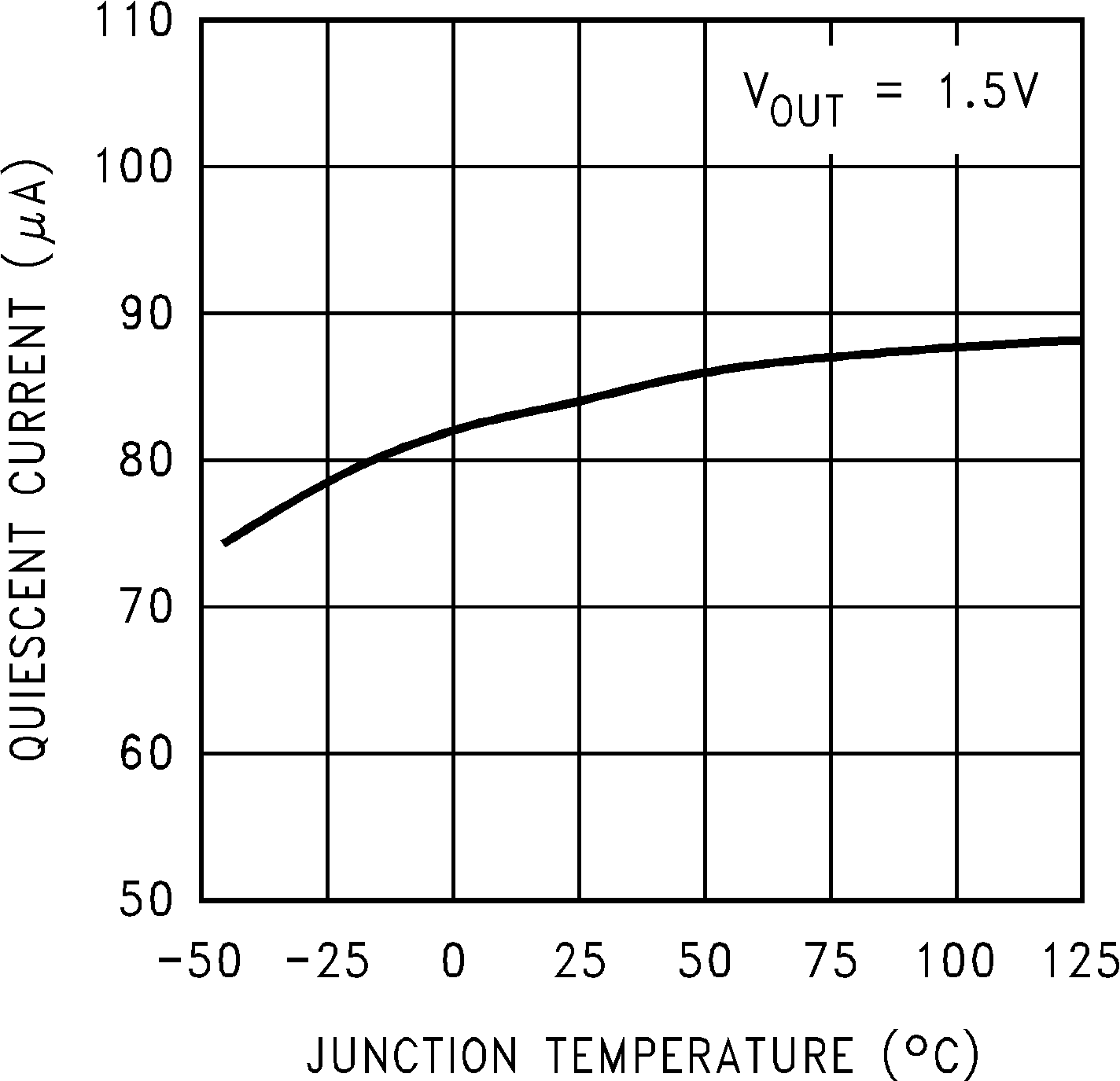
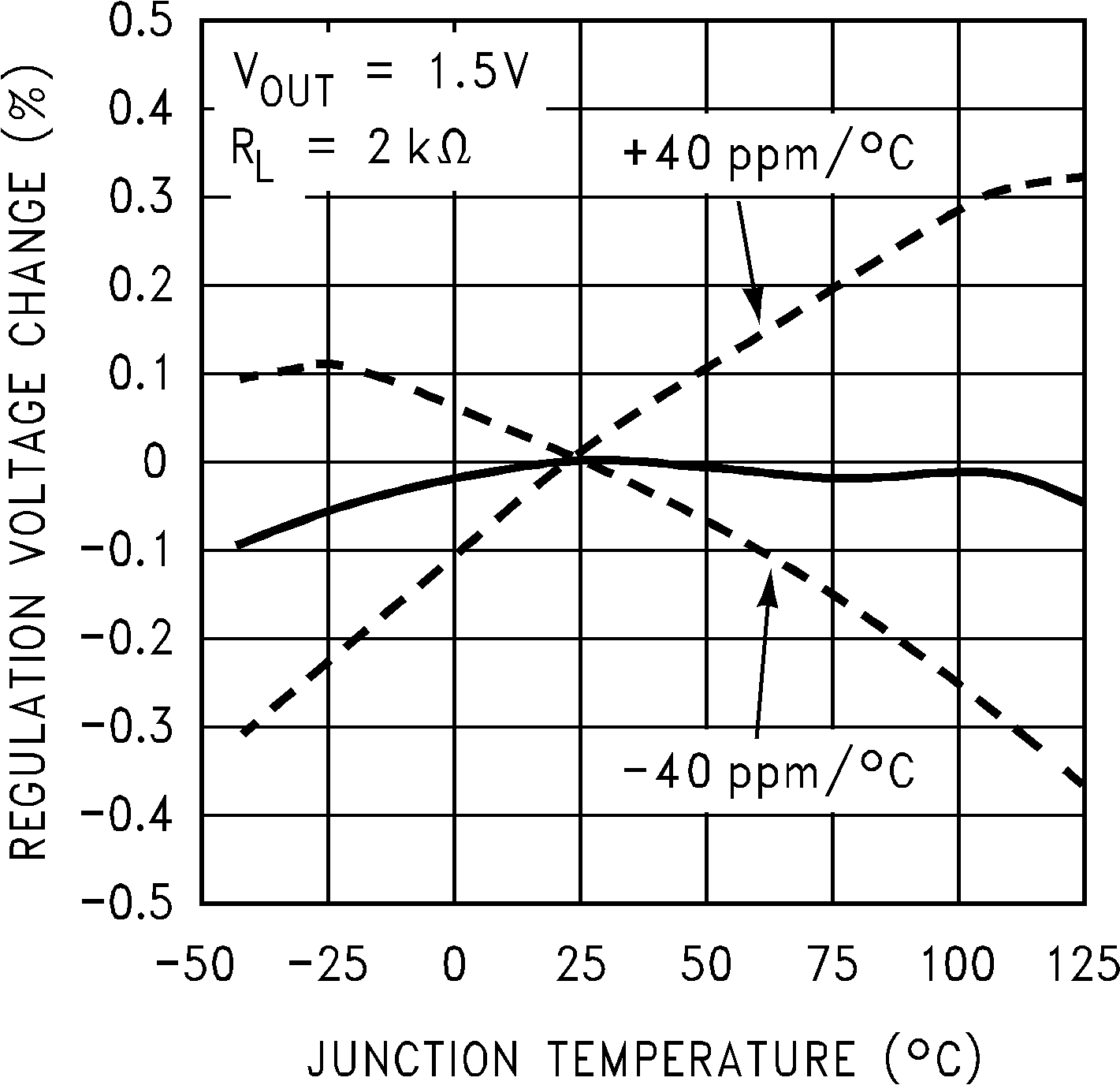
6.7 Typical Characteristics