SNVS116E May 1998 – December 2014 LM3420
PRODUCTION DATA.
- 1 Features
- 2 Applications
- 3 Description
- 4 Revision History
- 5 Pin Configuration and Functions
- 6 Specifications
- 7 Parameter Measurement Information
- 8 Detailed Description
-
9 Application and Implementation
- 9.1 Application Information
- 9.2
Typical Application: Constant Current/Constant Voltage Li-Ion Battery Charger
- 9.2.1 Design Requirements
- 9.2.2 Detailed Design Procedure
- 9.2.3 Application Curve
- 9.2.4
Other Application Circuits
- 9.2.4.1 Low Dropout Constant Current/Constant Voltage 2-Cell Charger
- 9.2.4.2 High-Efficiency Switching Regulator Constant Current/Constant Voltage 2-Cell Charger
- 9.2.4.3 Low Dropout Constant Current/Constant Voltage Li-Ion Battery Charger
- 9.2.4.4 High-Efficiency Switching Charger With High Side Current Sensing
- 9.2.4.5 Fast-Pulsed Constant Current 2-Cell Charger
- 9.2.4.6 MOSFET Low Dropout Charger
- 10Power Supply Recommendations
- 11Layout
- 12Device and Documentation Support
- 13Mechanical, Packaging, and Orderable Information
Package Options
Mechanical Data (Package|Pins)
- DBV|5
Thermal pad, mechanical data (Package|Pins)
Orderable Information
11 Layout
11.1 Layout Guidelines
For best overall performance, place all the circuit components on the same side of the circuit board and as near as practical to the respective pin connections. Place ground return connections to the input and output capacitor, and to the regulator ground pin as close to each other as possible, connected by a wide, component-side, copper surface. The use of vias and long traces to create circuit connections is strongly discouraged and negatively affects system performance. This grounding and layout scheme minimizes inductive parasitic, and thereby reduces load-current transients, minimizes noise, and increases circuit stability. A ground reference plane is also recommended and is either embedded in the PCB itself or located on the bottom side of the PCB opposite the components. This reference plane serves to assure accuracy of the output voltage, shield noise, and behaves similar to a thermal plane to spread heat from the device. In most applications, this ground plane is necessary to meet thermal requirements.
11.2 Layout Example
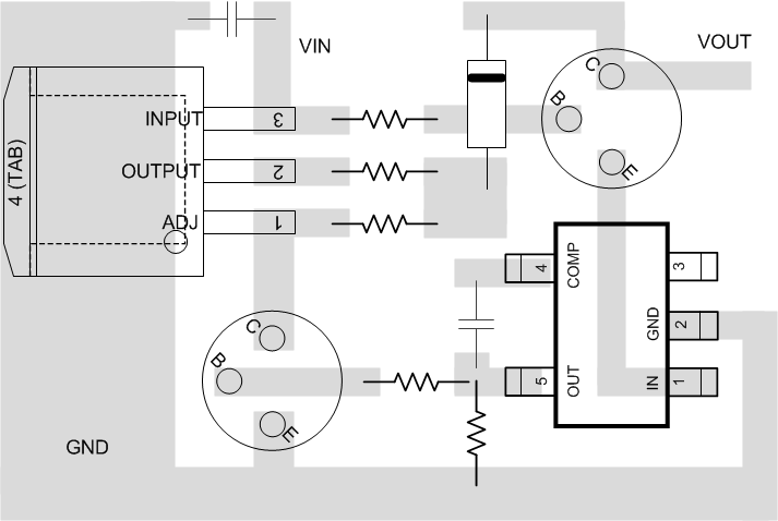 Figure 22. LM3420 Layout