SLOS456P January 2005 – March 2025
PRODUCTION DATA
- 1
- 1 Features
- 2 Applications
- 3 Description
- 4 Device Comparison Table
- 5 Pin Configuration and Functions
-
6 Specifications
- 6.1 Absolute Maximum Ratings
- 6.2 ESD Ratings
- 6.3 Recommended Operating Conditions
- 6.4 Thermal Information
- 6.5 LM4040A20I, LM4040B20I Electrical Characteristics
- 6.6 LM4040C20I, LM4040D20I Electrical Characteristics
- 6.7 LM4040C20Q, LM4040D20Q Electrical Characteristics
- 6.8 LM4040A25I, LM4040B25I Electrical Characteristics
- 6.9 LM4040C25I, LM4040D25I Electrical Characteristics
- 6.10 LM4040C25Q, LM4040D25Q Electrical Characteristics
- 6.11 LM4040A30I, LM4040B30I Electrical Characteristics
- 6.12 LM4040C30I, LM4040D30I Electrical Characteristics
- 6.13 LM4040C30Q, LM4040D30Q Electrical Characteristics
- 6.14 LM4040A41I, LM4040B41I Electrical Characteristics
- 6.15 LM4040C41I, LM4040D41I Electrical Characteristics
- 6.16 LM4040A50I, LM4040B50I Electrical Characteristics
- 6.17 LM4040C50I, LM4040D50I Electrical Characteristics
- 6.18 LM4040C50Q, LM4040D50Q Electrical Characteristics
- 6.19 LM4040A82I, LM4040B82I Electrical Characteristics
- 6.20 LM4040C82I, LM4040D82I Electrical Characteristics
- 6.21 LM4040A10I, LM4040B10I Electrical Characteristics
- 6.22 LM4040C10I, LM4040D10I Electrical Characteristics
- 6.23 Typical Characteristics
- 7 Detailed Description
- 8 Applications and Implementation
- 9 Device and Documentation Support
- 10Revision History
- 11Mechanical, Packaging, and Orderable Information
Package Options
Mechanical Data (Package|Pins)
Thermal pad, mechanical data (Package|Pins)
Orderable Information
8.2.2.2 Cathode and Load Currents
In a typical shunt-regulator configuration (see Figure 8-2), an external resistor, RS, is connected between the supply and the cathode of the LM4040. RS must be set properly, as RS sets the total current available to supply the load (IL) and bias the LM4040 (IZ). In all cases, IZ must stay within a specified range for proper operation of the reference. Taking into consideration one extreme in the variation of the load and supply voltage (maximum IL and minimum VS), RS must be small enough to supply the minimum IZ required for operation of the regulator, as given by data-sheet parameters. At the other extreme, maximum VS and minimum IL, RS must be large enough to limit IZ to less than the maximum-rated value of 15mA.
RS is calculated according to Equation 1:
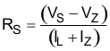
 Figure 8-2 Shunt Regulator