SLVSFF1C December 2021 – November 2025 LM5123-Q1
PRODUCTION DATA
- 1
- 1 Features
- 2 Applications
- 3 Description
- 4 Description (continued)
- 5 Pin Configuration and Functions
- 6 Specifications
-
7 Detailed Description
- 7.1 Overview
- 7.2 Functional Block Diagram
- 7.3
Feature Description
- 7.3.1 Device Enable/Disable (EN, VH Pin)
- 7.3.2 High Voltage VCC Regulator (BIAS, VCC Pin)
- 7.3.3 Light Load Switching Mode Selection (MODE Pin)
- 7.3.4 VOUT Range Selection (RANGE Pin)
- 7.3.5 Line Undervoltage Lockout (UVLO Pin)
- 7.3.6 Fast Restart Using VCC HOLD (VH Pin)
- 7.3.7 Adjustable Output Regulation Target (VOUT, TRK, VREF Pin)
- 7.3.8 Overvoltage Protection (VOUT Pin)
- 7.3.9 Power Good Indicator (PGOOD Pin)
- 7.3.10 Dynamically Programmable Switching Frequency (RT)
- 7.3.11 External Clock Synchronization (SYNC Pin)
- 7.3.12 Programmable Spread Spectrum (DITHER Pin)
- 7.3.13 Programmable Soft Start (SS Pin)
- 7.3.14 Wide Bandwidth Transconductance Error Amplifier and PWM (TRK, COMP Pin)
- 7.3.15 Current Sensing and Slope Compensation (CSP, CSN Pin)
- 7.3.16 Constant Peak Current Limit (CSP, CSN Pin)
- 7.3.17 Maximum Duty Cycle and Minimum Controllable On-Time Limits
- 7.3.18 Deep Sleep Mode and Bypass Operation (HO, CP Pin)
- 7.3.19 MOSFET Drivers, Integrated Boot Diode, and Hiccup Mode Fault Protection (LO, HO, HB Pin)
- 7.3.20 Thermal Shutdown Protection
- 7.4 Device Functional Modes
- 8 Application and Implementation
- 9 Power Supply Recommendations
- 10Layout
- 11Device and Documentation Support
- 12Revision History
- 13Mechanical, Packaging, and Orderable Information
Package Options
Refer to the PDF data sheet for device specific package drawings
Mechanical Data (Package|Pins)
- RGR|20
Thermal pad, mechanical data (Package|Pins)
- RGR|20
Orderable Information
7.3.16 Constant Peak Current Limit (CSP, CSN Pin)
When the CSP-CSN voltage exceeds the 60mV cycle-by-cycle current limit threshold (VCLTH), the current limit comparator immediately terminates the LO output. The device provides an constant peak current limit whose peak inductor current limit is constant over the input and output voltage. For the case where the inductor current can overshoot, such as inductor saturation, the current limit comparator skips pulses until the current has decayed below the current limit threshold.
 Figure 7-15 Current Limit Comparator
Cycle-by-cycle peak current limit is calculated as follows:
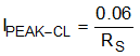
 Figure 7-16 Current Limit Comparator Input
 Boost converters have a natural pass-through path from the supply to the load through the high-side MOSFET body diode. Due to this path, boost converters cannot provide the peak current limit protection when the output voltage is close to or less than the input supply voltage, especially the peak current limit protection that does not work during the minimum on time (tON-MIN).