SNVSA47D February 2016 – December 2022 LM5165
PRODUCTION DATA
- 1 Features
- 2 Applications
- 3 Description
- 4 Revision History
- 5 Pin Configuration and Functions
- 6 Specifications
-
7 Detailed Description
- 7.1 Overview
- 7.2 Functional Block Diagram
- 7.3
Feature Description
- 7.3.1 Integrated Power MOSFETs
- 7.3.2 Selectable PFM or COT Mode Converter Operation
- 7.3.3 COT Mode Light-Load Operation
- 7.3.4 Low Dropout Operation and 100% Duty Cycle Mode
- 7.3.5 Adjustable Output Voltage (FB)
- 7.3.6 Adjustable Current Limit
- 7.3.7 Precision Enable (EN) and Hysteresis (HYS)
- 7.3.8 Power Good (PGOOD)
- 7.3.9 Configurable Soft Start (SS)
- 7.3.10 Thermal Shutdown
- 7.4 Device Functional Modes
-
8 Applications and Implementation
- 8.1 Application Information
- 8.2
Typical Applications
- 8.2.1 Design 1: Wide VIN, Low IQ COT Converter Rated at 5 V, 150 mA
- 8.2.2 Design 2: Small Solution Size PFM Converter Rated at 3.3 V, 50 mA
- 8.2.3 Design 3: High Density 12-V, 75-mA PFM Converter
- 8.2.4 Design 4: 3.3-V, 150-mA COT Converter With High Efficiency
- 8.2.5 Design 5: 15-V, 150-mA, 600-kHz COT Converter
- 8.3 Power Supply Recommendations
- 8.4 Layout
- 9 Device and Documentation Support
- 10Mechanical, Packaging, and Orderable Information
Package Options
Mechanical Data (Package|Pins)
- DRC|10
Thermal pad, mechanical data (Package|Pins)
- DRC|10
Orderable Information
8.2.1.2.3 Filter Inductor – LF
Added additional statement to inductor selection in applications section.
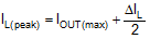
The inductor ripple current (assuming CCM operation) and peak inductor current are given respectively by Equation 11 and Equation 12.
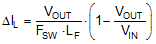
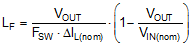
For most applications, choose an inductance such that the inductor ripple current, ΔIL, is between 30% and 50% of the rated load current at nominal input voltage. Calculate the inductance using Equation 13.
Choosing a 220-µH inductor in this design results in 55-mA peak-to-peak ripple current at nominal input voltage of 12 V, equivalent to 37% of the 150-mA rated load current. The peak inductor current at maximum input voltage of 65 V is 195 mA, sufficiently below the LM5165 peak current limit of 240 mA.
The inductors selected for the following designs were meant for nominal operating conditions, and component behavior can deviate from expected results in situations like over current. Check the inductor data sheet to ensure that the inductor saturation current is well above the current limit setting of a particular design. Ferrite designs have low core loss and are preferred at high switching frequencies, so design goals can then concentrate on copper loss and preventing saturation. However, ferrite core materials exhibit a hard saturation characteristic – the inductance collapses abruptly when the saturation current is exceeded. This results in an abrupt increase in inductor ripple current, higher output voltage ripple, not to mention reduced efficiency and compromised reliability. Note that inductor saturation current generally deceases as the core temperature increases.