SNVSA47D February   2016  – December 2022 LM5165

PRODUCTION DATA  

  1. Features
  2. Applications
  3. Description
  4. Revision History
  5. Pin Configuration and Functions
  6. Specifications
    1. 6.1 Absolute Maximum Ratings
    2. 6.2 ESD Ratings
    3. 6.3 Recommended Operating Conditions
    4. 6.4 Thermal Information
    5. 6.5 Electrical Characteristics
    6. 6.6 Switching Characteristics
    7. 6.7 Typical Characteristics
  7. Detailed Description
    1. 7.1 Overview
    2. 7.2 Functional Block Diagram
    3. 7.3 Feature Description
      1. 7.3.1  Integrated Power MOSFETs
      2. 7.3.2  Selectable PFM or COT Mode Converter Operation
      3. 7.3.3  COT Mode Light-Load Operation
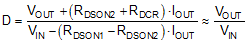
      4. 7.3.4  Low Dropout Operation and 100% Duty Cycle Mode
      5. 7.3.5  Adjustable Output Voltage (FB)
      6. 7.3.6  Adjustable Current Limit
      7. 7.3.7  Precision Enable (EN) and Hysteresis (HYS)
      8. 7.3.8  Power Good (PGOOD)
      9. 7.3.9  Configurable Soft Start (SS)
      10. 7.3.10 Thermal Shutdown
    4. 7.4 Device Functional Modes
      1. 7.4.1 Shutdown Mode
      2. 7.4.2 Standby Mode
      3. 7.4.3 Active Mode in COT
      4. 7.4.4 Active Mode in PFM
      5. 7.4.5 Sleep Mode in PFM
  8. Applications and Implementation
    1. 8.1 Application Information
    2. 8.2 Typical Applications
      1. 8.2.1 Design 1: Wide VIN, Low IQ COT Converter Rated at 5 V, 150 mA
        1. 8.2.1.1 Design Requirements
        2. 8.2.1.2 Detailed Design Procedure
          1. 8.2.1.2.1 Custom Design With WEBENCH® Tools
          2. 8.2.1.2.2 Switching Frequency – RT
          3. 8.2.1.2.3 Filter Inductor – LF
          4. 8.2.1.2.4 Output Capacitors – COUT
          5. 8.2.1.2.5 Series Ripple Resistor – RESR
          6. 8.2.1.2.6 Input Capacitor – CIN
          7. 8.2.1.2.7 Soft-Start Capacitor – CSS
        3. 8.2.1.3 Application Curves
      2. 8.2.2 Design 2: Small Solution Size PFM Converter Rated at 3.3 V, 50 mA
        1. 8.2.2.1 Design Requirements
        2. 8.2.2.2 Detailed Design Procedure
          1. 8.2.2.2.1 Peak Current Limit Setting – RILIM
          2. 8.2.2.2.2 Switching Frequency – LF
          3. 8.2.2.2.3 Output Capacitor – COUT
          4. 8.2.2.2.4 Input Capacitor – CIN
        3. 8.2.2.3 Application Curves
      3. 8.2.3 Design 3: High Density 12-V, 75-mA PFM Converter
        1. 8.2.3.1 Design Requirements
        2. 8.2.3.2 Detailed Design Procedure
          1. 8.2.3.2.1 Peak Current Limit Setting – RILIM
          2. 8.2.3.2.2 Switching Frequency – LF
          3. 8.2.3.2.3 Input and Output Capacitors – CIN, COUT
          4. 8.2.3.2.4 Feedback Resistors – RFB1, RFB2
          5. 8.2.3.2.5 Undervoltage Lockout Setpoint – RUV1, RUV2, RHYS
          6. 8.2.3.2.6 Soft Start – CSS
        3. 8.2.3.3 Application Curves
      4. 8.2.4 Design 4: 3.3-V, 150-mA COT Converter With High Efficiency
        1. 8.2.4.1 Design Requirements
        2. 8.2.4.2 Application Curves
      5. 8.2.5 Design 5: 15-V, 150-mA, 600-kHz COT Converter
        1. 8.2.5.1 Design Requirements
        2. 8.2.5.2 Detailed Design Procedure
          1. 8.2.5.2.1 COT Output Ripple Voltage Reduction
        3. 8.2.5.3 Application Curves
    3. 8.3 Power Supply Recommendations
    4. 8.4 Layout
      1. 8.4.1 Layout Guidelines
        1. 8.4.1.1 Compact PCB Layout for EMI Reduction
        2. 8.4.1.2 Feedback Resistor Layout
      2. 8.4.2 Layout Example
  9. Device and Documentation Support
    1. 9.1 Device Support
      1. 9.1.1 Third-Party Products Disclaimer
      2. 9.1.2 Development Support
      3. 9.1.3 Custom Design With WEBENCH® Tools
    2. 9.2 Documentation Support
      1. 9.2.1 Related Documentation
    3. 9.3 Receiving Notification of Documentation Updates
    4. 9.4 Support Resources
    5. 9.5 Trademarks
    6. 9.6 Electrostatic Discharge Caution
    7. 9.7 Glossary
  10. 10Mechanical, Packaging, and Orderable Information

Package Options

Mechanical Data (Package|Pins)
Thermal pad, mechanical data (Package|Pins)
Orderable Information

Low Dropout Operation and 100% Duty Cycle Mode

If RDSON1 and RDSON2 are the high-side and low-side MOSFET on-state resistances, respectively, and RDCR is the inductor DC resistance, the duty cycle in COT (CCM) or PFM mode is given by Equation 3.

Equation 3. GUID-E622C8AB-132B-4D8D-8CF8-1010CF8EE67F-low.gif

The LM5165 offers a low input voltage to output voltage dropout by engaging the high-side MOSFET at 100% duty cycle. In COT mode, a frequency foldback feature effectively extends maximum duty cycle to 100% during low dropout conditions or load-on transients. Based on the 4-mV FB comparator dropout hysteresis, the duty cycle extends as needed at low input voltage conditions, corresponding to lower switching frequency. The PWM on-time extends based on the requirement that the FB voltage exceeds the dropout hysteresis during a given on-time. 100% duty cycle operation is eventually reached as the input voltage decreases towards the output setpoint. The output voltage stays in regulation at a lower supply voltage, thus achieving an extremely low dropout voltage.

Note that PFM mode operation provides an inherently natural transition to 100% duty cycle if needed for low dropout applications.

Use Equation 4 to calculate the minimum input voltage to maintain output regulation.

Equation 4. GUID-A7C24683-5B35-4DB2-B640-9BEAA323849E-low.gif