SNVSA47D February 2016 – December 2022 LM5165
PRODUCTION DATA
- 1 Features
- 2 Applications
- 3 Description
- 4 Revision History
- 5 Pin Configuration and Functions
- 6 Specifications
-
7 Detailed Description
- 7.1 Overview
- 7.2 Functional Block Diagram
- 7.3
Feature Description
- 7.3.1 Integrated Power MOSFETs
- 7.3.2 Selectable PFM or COT Mode Converter Operation
- 7.3.3 COT Mode Light-Load Operation
- 7.3.4 Low Dropout Operation and 100% Duty Cycle Mode
- 7.3.5 Adjustable Output Voltage (FB)
- 7.3.6 Adjustable Current Limit
- 7.3.7 Precision Enable (EN) and Hysteresis (HYS)
- 7.3.8 Power Good (PGOOD)
- 7.3.9 Configurable Soft Start (SS)
- 7.3.10 Thermal Shutdown
- 7.4 Device Functional Modes
-
8 Applications and Implementation
- 8.1 Application Information
- 8.2
Typical Applications
- 8.2.1 Design 1: Wide VIN, Low IQ COT Converter Rated at 5 V, 150 mA
- 8.2.2 Design 2: Small Solution Size PFM Converter Rated at 3.3 V, 50 mA
- 8.2.3 Design 3: High Density 12-V, 75-mA PFM Converter
- 8.2.4 Design 4: 3.3-V, 150-mA COT Converter With High Efficiency
- 8.2.5 Design 5: 15-V, 150-mA, 600-kHz COT Converter
- 8.3 Power Supply Recommendations
- 8.4 Layout
- 9 Device and Documentation Support
- 10Mechanical, Packaging, and Orderable Information
Package Options
Mechanical Data (Package|Pins)
- DRC|10
Thermal pad, mechanical data (Package|Pins)
- DRC|10
Orderable Information
7.3.2 Selectable PFM or COT Mode Converter Operation
Figure 7-1 and Figure 7-2 show converter schematics for PFM and COT modes of operation.
 Fixed Output Voltage of 5 V or 3.3 V, (b) Adjustable Output Voltage With Programmable Soft Start, Current Limit, and UVLO") Figure 7-1 PFM Mode Converter Schematics: (a) Fixed Output Voltage of 5 V or 3.3 V, (b) Adjustable Output Voltage With Programmable Soft Start, Current Limit, and UVLO
Figure 7-1 PFM Mode Converter Schematics: (a) Fixed Output Voltage of 5 V or 3.3 V, (b) Adjustable Output Voltage With Programmable Soft Start, Current Limit, and UVLO Fixed Output Voltage of 5 V or 3.3 V, (b) Adjustable Output Voltage With Programmable Soft Start, Current Limit, and UVLO") Figure 7-2 COT Mode Converter Schematics: (a) Fixed Output Voltage of 5 V or 3.3 V, (b) Adjustable Output Voltage With Programmable Soft Start, Current Limit, and UVLO
Figure 7-2 COT Mode Converter Schematics: (a) Fixed Output Voltage of 5 V or 3.3 V, (b) Adjustable Output Voltage With Programmable Soft Start, Current Limit, and UVLOThe LM5165 operates in PFM mode when RT is shorted to GND. Configured as such, the LM5165 behaves as a hysteretic voltage regulator operating in boundary conduction mode, controlling the output voltage within upper and lower hysteresis levels according to the PFM feedback comparator hysteresis of 10 mV. Figure 7-3 is a representation of the relevant output voltage and inductor current waveforms. The LM5165 provides the required switching pulses to recharge the output capacitor, followed by a sleep period where most of the internal circuits are shut off. The load current is supported by the output capacitor during this time, and the LM5165 current consumption approaches the sleep quiescent current of 10.5 µA. The sleep period duration depends on load current and output capacitance.
When operating in PFM mode at given input and output voltages, the chosen filter inductance dictates the PFM pulse frequency in Equation 1:
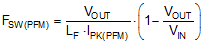
where
- IPK(PFM) corresponds to one of the four programmable levels for peak limit of inductor current. See Adjustable Current Limit for more detail.
Configured in COT mode, the LM5165 based converter turns on the high-side MOSFET with on-time inversely proportional to VIN to operate with essentially fixed switching frequency when in continuous conduction mode (CCM). Diode emulation mode (DEM) prevents negative inductor current, and pulse skipping maintains highest efficiency at light load currents by decreasing the effective switching frequency. The COT-controlled LM5165 waveforms in CCM and DEM are represented in Figure 7-4. The PWM on-time is set by resistor RRT connected from RT to GND as shown in Figure 7-2. The control loop maintains a constant output voltage by adjusting the PWM off-time.
The required on-time adjust resistance for a particular frequency is given in Equation 2 and tabulated in Table 7-1. The maximum programmable on-time is 15 µs.
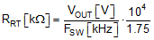
| FSW (kHz) | RRT (kΩ) | |||
|---|---|---|---|---|
| VOUT = 1.8 V | VOUT = 3.3 V | VOUT = 5 V | VOUT = 12 V | |
| 100 | 102 | 187 | 287 | 681 |
| 200 | 51.1 | 95.3 | 143 | 240 |
| 300 | 34 | 63.4 | 95.3 | 226 |
| 400 | 25.5 | 47.5 | 71.5 | 169 |
| 500 | 20.5 | 37.4 | 57.6 | 137 |
| 600 | 16.9 | 31.6 | 47.5 | 115 |
The choice of control mode and switching frequency requires a compromise between conversion efficiency, quiescent current, and passive component size. Lower switching frequency implies reduced switching losses (including gate charge losses, transition losses, and so forth) and higher overall efficiency. Higher switching frequency, on the other hand, implies a smaller LC output filter and hence a more compact design. Lower inductance also helps transient response as the large-signal slew rate of inductor current increases. The ideal switching frequency in a given application is a tradeoff and thus is determined on a case-by-case basis. It relates to the input voltage, output voltage, most frequent load current level(s), external component choices, and circuit size requirement. At light loads, the PFM converter has a relatively longer sleep time interval and thus operates with lower input quiescent current and higher efficiency.