SNOSD87A July 2021 – February 2022 LM74501-Q1
PRODUCTION DATA
- 1 Features
- 2 Applications
- 3 Description
- 4 Revision History
- 5 Pin Configuration and Functions
- 6 Specifications
- 7 Parameter Measurement Information
- 8 Detailed Description
- 9 Application and Implementation
- 10Power Supply Recommendations
- 11Layout
- 12Device and Documentation Support
- 13Mechanical, Packaging, and Orderable Information
Package Options
Mechanical Data (Package|Pins)
- DDF|8
Thermal pad, mechanical data (Package|Pins)
Orderable Information
3 Description
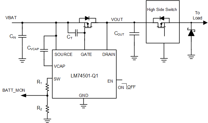
The LM74501-Q1 operates in conjunction with an external N-channel MOSFET as a low loss reverse polarity protection solution. The device supports wide supply input range of 3.2 V to 65 V. The 3.2-V input voltage support is particularly well suited for severe cold crank requirements in automotive systems. The device can withstand and protect the loads from negative supply voltages down to –18 V. The LM74501-Q1 does not have reverse current blocking functionality and is suitable for input reverse polarity protection of loads that can potentially deliver energy back to the input supply such as automotive body control module motor loads.
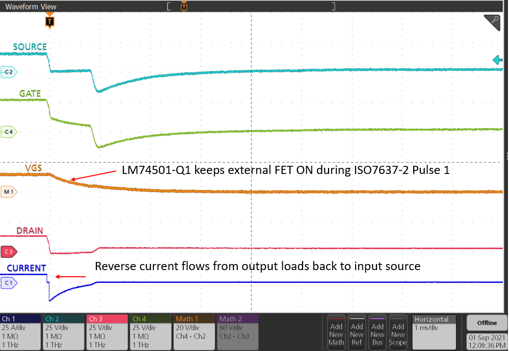
The LM74501-Q1 controller provides a charge pump gate drive for an external N-channel MOSFET. The LM74501-Q1 has a unique integrated feature that allows systems to meet automotive ISO7637 pulse 1 transient requirements without an additional TVS Diode (TVS less). The LM74501-Q1 features an integrated switch to enable battery voltage monitoring with an external resistor divider. With the enable pin low, the controller is off and draws only around 1 µA of current, thus offering low system current when put into sleep mode.
| PART NUMBER | PACKAGE(1) | BODY SIZE (NOM) |
|---|---|---|
| LM74501-Q1 | SOT-23 (8) | 2.90 mm × 1.60 mm |
 LM74501-Q1 Typical Application Schematic for Automotive Battery Reverse Polarity Protection
 TVS Less
ISO7637-2 Pulse 1 Operation