SNVSBK5A February 2020 – July 2020 LM76005
PRODUCTION DATA
- 1 Features
- 2 Applications
- 3 Description
- 4 Revision History
- 5 Pin Configuration and Functions
- 6 Specifications
-
7 Detailed Description
- 7.1 Overview
- 7.2 Functional Block Diagram
- 7.3
Feature Description
- 7.3.1 Fixed-Frequency, Peak-Current-Mode Control
- 7.3.2 Light Load Operation Modes — PFM and FPWM
- 7.3.3 Adjustable Output Voltage
- 7.3.4 Enable (EN Pin) and UVLO
- 7.3.5 Internal LDO, VCC UVLO, and Bias Input
- 7.3.6 Soft Start and Voltage Tracking (SS/TRK)
- 7.3.7 Adjustable Switching Frequency (RT) and Frequency Synchronization
- 7.3.8 Minimum On-Time, Minimum Off-Time, and Frequency Foldback at Dropout Conditions
- 7.3.9 Bootstrap Voltage and VBOOT UVLO (BOOT Pin)
- 7.3.10 Power Good and Overvoltage Protection (PGOOD)
- 7.3.11 Overcurrent and Short-Circuit Protection
- 7.3.12 Thermal Shutdown
- 7.4 Device Functional Modes
-
8 Application and Implementation
- 8.1 Application Information
- 8.2
Typical Applications
- 8.2.1 Design Requirements
- 8.2.2
Detailed Design Procedure
- 8.2.2.1 Custom Design With WEBENCH® Tools
- 8.2.2.2 Output Voltage Setpoint
- 8.2.2.3 Switching Frequency
- 8.2.2.4 Input Capacitors
- 8.2.2.5 Inductor Selection
- 8.2.2.6 Output Capacitor Selection
- 8.2.2.7 Feedforward Capacitor
- 8.2.2.8 Bootstrap Capacitors
- 8.2.2.9 VCC Capacitors
- 8.2.2.10 BIAS Capacitors
- 8.2.2.11 Soft-Start Capacitors
- 8.2.2.12 Undervoltage Lockout Setpoint
- 8.2.2.13 PGOOD
- 8.2.2.14 Synchronization
- 8.2.3 Application Curves
- 9 Power Supply Recommendations
- 10Layout
- 11Device and Documentation Support
- 12Mechanical, Packaging, and Orderable Information
Package Options
Mechanical Data (Package|Pins)
- RNP|30
Thermal pad, mechanical data (Package|Pins)
- RNP|30
Orderable Information
8.2.2.6 Output Capacitor Selection
The device is designed to be used with a wide variety of LC filters. TI generally recommends using as little output capacitance as possible to keep cost and size down. Choose the output capacitor or capacitors, COUT, with care as it directly affects the steady-state output-voltage ripple, loop stability, and the voltage over/undershoot during load current transients.
The output voltage ripple is essentially composed of two parts. One is caused by the inductor current ripple going through the equivalent series resistance (ESR) of the output capacitors:
The other is caused by the inductor current ripple charging and discharging the output capacitors:
The two components in the voltage ripple are not in phase, so the actual peak-to-peak ripple is smaller than the sum of the two peaks.
Output capacitance is usually limited by transient performance specifications if the system requires tight voltage regulation in the presence of large current steps and fast slew rates. When a fast large load transient happens, output capacitors provide the required charge before the inductor current can slew to the appropriate level. The initial output voltage step is equal to the load current step multiplied by the ESR. VOUT continues to droop until the control loop response increases or decreases the inductor current to supply the load. To maintain a small overshoot or undershoot during a transient, small ESR, and large capacitance are desired. But these also come with higher cost and size. Thus, the motivation is to seek a fast control loop response to reduce the output voltage deviation.
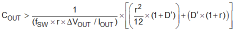
For a given input and output requirement, Equation 20 gives an approximation for an absolute minimum output cap required:
Along with this for the same requirement, calculate the maximum ESR as per Equation 21:
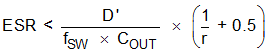
where
- r = ripple ratio of the inductor ripple current (ΔiL / IOUT)
- ΔVO = target output voltage undershoot
- D’ = 1 – duty cycle
- fSW = switching frequency
- IOUT = load current
A general guideline for COUT range is that COUT must be larger than the minimum required output capacitance calculated by Equation 20. Limit the maximum value of total output capacitance to between 800 μF and 1200 μF. Large values of output capacitance can prevent the regulator from starting up correctly and adversely effect the loop stability. If values greater than the given range are to be used, then a careful study of start-up at full load and loop stability must be performed.
In applications with VOUT less than 3.3 V, it is critical that low ESR output capacitors are selected. This limits potential output voltage overshoots as the input voltage falls below the device normal operating range. To optimize the transient behavior a feedforward capacitor can be added in parallel with the upper feedback resistor. For this design example, three 47-µF, 10-V, X7R ceramic capacitors are used in parallel.