SNVSBK5A February 2020 – July 2020 LM76005
PRODUCTION DATA
- 1 Features
- 2 Applications
- 3 Description
- 4 Revision History
- 5 Pin Configuration and Functions
- 6 Specifications
-
7 Detailed Description
- 7.1 Overview
- 7.2 Functional Block Diagram
- 7.3
Feature Description
- 7.3.1 Fixed-Frequency, Peak-Current-Mode Control
- 7.3.2 Light Load Operation Modes — PFM and FPWM
- 7.3.3 Adjustable Output Voltage
- 7.3.4 Enable (EN Pin) and UVLO
- 7.3.5 Internal LDO, VCC UVLO, and Bias Input
- 7.3.6 Soft Start and Voltage Tracking (SS/TRK)
- 7.3.7 Adjustable Switching Frequency (RT) and Frequency Synchronization
- 7.3.8 Minimum On-Time, Minimum Off-Time, and Frequency Foldback at Dropout Conditions
- 7.3.9 Bootstrap Voltage and VBOOT UVLO (BOOT Pin)
- 7.3.10 Power Good and Overvoltage Protection (PGOOD)
- 7.3.11 Overcurrent and Short-Circuit Protection
- 7.3.12 Thermal Shutdown
- 7.4 Device Functional Modes
-
8 Application and Implementation
- 8.1 Application Information
- 8.2
Typical Applications
- 8.2.1 Design Requirements
- 8.2.2
Detailed Design Procedure
- 8.2.2.1 Custom Design With WEBENCH® Tools
- 8.2.2.2 Output Voltage Setpoint
- 8.2.2.3 Switching Frequency
- 8.2.2.4 Input Capacitors
- 8.2.2.5 Inductor Selection
- 8.2.2.6 Output Capacitor Selection
- 8.2.2.7 Feedforward Capacitor
- 8.2.2.8 Bootstrap Capacitors
- 8.2.2.9 VCC Capacitors
- 8.2.2.10 BIAS Capacitors
- 8.2.2.11 Soft-Start Capacitors
- 8.2.2.12 Undervoltage Lockout Setpoint
- 8.2.2.13 PGOOD
- 8.2.2.14 Synchronization
- 8.2.3 Application Curves
- 9 Power Supply Recommendations
- 10Layout
- 11Device and Documentation Support
- 12Mechanical, Packaging, and Orderable Information
Package Options
Mechanical Data (Package|Pins)
- RNP|30
Thermal pad, mechanical data (Package|Pins)
- RNP|30
Orderable Information
8.2.2.3 Switching Frequency
The default switching frequency of the LM76005 device is set at 400 kHz. If the RT is left open, the LM76005 switches at 400 kHz in CCM mode. Use Equation 13 to calculate the required value for RT to operate the LM76005 at different frequencies.
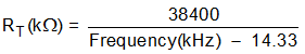
The result for 400 kHz is 99.57 kΩ.
The choice of switching frequency is a compromise between conversion efficiency and overall solution size. Lower switching frequency implies reduced switching losses and usually results in higher system efficiency. However, higher switching frequency allows for the use of smaller inductors and output capacitors, hence, a more compact design. When choosing operating frequency, the most important consideration is thermal limitations. This constraint typically dominates frequency selection. For the LM76005, the safe operating area is controlled by the thermal performance (RθJA=18.8 °C/W); see Figure 8-3.
") Figure 8-3 LM76005 Safe Operating Area (5 VOUT, 400 kHz, RθJA=18.8 °C/W)
Figure 8-3 LM76005 Safe Operating Area (5 VOUT, 400 kHz, RθJA=18.8 °C/W)