SNVSBK5A February 2020 – July 2020 LM76005
PRODUCTION DATA
- 1 Features
- 2 Applications
- 3 Description
- 4 Revision History
- 5 Pin Configuration and Functions
- 6 Specifications
-
7 Detailed Description
- 7.1 Overview
- 7.2 Functional Block Diagram
- 7.3
Feature Description
- 7.3.1 Fixed-Frequency, Peak-Current-Mode Control
- 7.3.2 Light Load Operation Modes — PFM and FPWM
- 7.3.3 Adjustable Output Voltage
- 7.3.4 Enable (EN Pin) and UVLO
- 7.3.5 Internal LDO, VCC UVLO, and Bias Input
- 7.3.6 Soft Start and Voltage Tracking (SS/TRK)
- 7.3.7 Adjustable Switching Frequency (RT) and Frequency Synchronization
- 7.3.8 Minimum On-Time, Minimum Off-Time, and Frequency Foldback at Dropout Conditions
- 7.3.9 Bootstrap Voltage and VBOOT UVLO (BOOT Pin)
- 7.3.10 Power Good and Overvoltage Protection (PGOOD)
- 7.3.11 Overcurrent and Short-Circuit Protection
- 7.3.12 Thermal Shutdown
- 7.4 Device Functional Modes
-
8 Application and Implementation
- 8.1 Application Information
- 8.2
Typical Applications
- 8.2.1 Design Requirements
- 8.2.2
Detailed Design Procedure
- 8.2.2.1 Custom Design With WEBENCH® Tools
- 8.2.2.2 Output Voltage Setpoint
- 8.2.2.3 Switching Frequency
- 8.2.2.4 Input Capacitors
- 8.2.2.5 Inductor Selection
- 8.2.2.6 Output Capacitor Selection
- 8.2.2.7 Feedforward Capacitor
- 8.2.2.8 Bootstrap Capacitors
- 8.2.2.9 VCC Capacitors
- 8.2.2.10 BIAS Capacitors
- 8.2.2.11 Soft-Start Capacitors
- 8.2.2.12 Undervoltage Lockout Setpoint
- 8.2.2.13 PGOOD
- 8.2.2.14 Synchronization
- 8.2.3 Application Curves
- 9 Power Supply Recommendations
- 10Layout
- 11Device and Documentation Support
- 12Mechanical, Packaging, and Orderable Information
Package Options
Mechanical Data (Package|Pins)
- RNP|30
Thermal pad, mechanical data (Package|Pins)
- RNP|30
Orderable Information
7.3.10 Power Good and Overvoltage Protection (PGOOD)
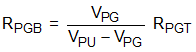
The LM76005 has a built-in power-good flag shown on the PGOOD pin to indicate whether the output voltage is within its regulation level. The PGOOD signal can be used for start-up sequencing of multiple rails. The PGOOD pin is an open-drain output that requires a pullup resistor to an appropriate logic voltage (any voltage below 12 V). The pin can sink 5 mA of current and maintain its specified logic low level. A typical range of pullup resistor value is 10 kΩ to 100 kΩ. When the FB voltage is outside the power-good band, +6% above and –7% below the internal reference VREF typically, the PGOOD switch is turned on, and the PGOOD pin voltage is pulled to ground. When the FB is 2.5% (typical) closer to FB than the PGOOD threshold, the PGOOD switch is turned off, and the pin is pulled up to the voltage connected to the pullup resistor. Both rising and falling edges of the power-good flag have a built-in 140-µs (typical) deglitch delay. To pull up the PGOOD pin to a voltage higher than 15 V, a resistor divider can be used to divide the voltage down.
 Figure 7-8 PGOOD Resistor Divider
For given pullup voltage, VPU, the desired voltage on PGOOD pin, VPG, and RPGT chosen, use Equation 11 to calculate RPGB: