SNVSBK5A February 2020 – July 2020 LM76005
PRODUCTION DATA
- 1 Features
- 2 Applications
- 3 Description
- 4 Revision History
- 5 Pin Configuration and Functions
- 6 Specifications
-
7 Detailed Description
- 7.1 Overview
- 7.2 Functional Block Diagram
- 7.3
Feature Description
- 7.3.1 Fixed-Frequency, Peak-Current-Mode Control
- 7.3.2 Light Load Operation Modes — PFM and FPWM
- 7.3.3 Adjustable Output Voltage
- 7.3.4 Enable (EN Pin) and UVLO
- 7.3.5 Internal LDO, VCC UVLO, and Bias Input
- 7.3.6 Soft Start and Voltage Tracking (SS/TRK)
- 7.3.7 Adjustable Switching Frequency (RT) and Frequency Synchronization
- 7.3.8 Minimum On-Time, Minimum Off-Time, and Frequency Foldback at Dropout Conditions
- 7.3.9 Bootstrap Voltage and VBOOT UVLO (BOOT Pin)
- 7.3.10 Power Good and Overvoltage Protection (PGOOD)
- 7.3.11 Overcurrent and Short-Circuit Protection
- 7.3.12 Thermal Shutdown
- 7.4 Device Functional Modes
-
8 Application and Implementation
- 8.1 Application Information
- 8.2
Typical Applications
- 8.2.1 Design Requirements
- 8.2.2
Detailed Design Procedure
- 8.2.2.1 Custom Design With WEBENCH® Tools
- 8.2.2.2 Output Voltage Setpoint
- 8.2.2.3 Switching Frequency
- 8.2.2.4 Input Capacitors
- 8.2.2.5 Inductor Selection
- 8.2.2.6 Output Capacitor Selection
- 8.2.2.7 Feedforward Capacitor
- 8.2.2.8 Bootstrap Capacitors
- 8.2.2.9 VCC Capacitors
- 8.2.2.10 BIAS Capacitors
- 8.2.2.11 Soft-Start Capacitors
- 8.2.2.12 Undervoltage Lockout Setpoint
- 8.2.2.13 PGOOD
- 8.2.2.14 Synchronization
- 8.2.3 Application Curves
- 9 Power Supply Recommendations
- 10Layout
- 11Device and Documentation Support
- 12Mechanical, Packaging, and Orderable Information
Package Options
Mechanical Data (Package|Pins)
- RNP|30
Thermal pad, mechanical data (Package|Pins)
- RNP|30
Orderable Information
7.3.3 Adjustable Output Voltage
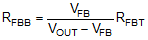
The voltage regulation loop in the LM76005 regulates the FB voltage to be the same as the internal reference voltage. The output voltage of the LM76005 is set by a resistor divider to program the ratio from VOUT to VFB. The resistor divider is connected from the output node to ground with the mid-point connecting to the FB pin.
 Figure 7-2 Output Voltage Setting
The voltage reference system produces a precise ±1% voltage reference over temperature. TI recommends using divider resistors with 1% tolerance or better with temperature coefficient of 100 ppm or lower. Selection of RFBT equal or lower than 100 kΩ is also recommended. RFBB can be calculated by Equation 1:
Larger RFBT and RFBB values reduce the current that goes through the divider, helping to increase light load efficiency. However, larger values also make the feedback path more susceptible to noise. If efficiency at very light load is not critical in a certain application, TI recommends RFBT = 10 kΩ to 100 kΩ. If the resistor divider is not connected properly, output voltage cannot be regulated because the feedback loop is broken. If the FB pin is shorted to ground or disconnected, the output voltage is driven close to VIN because the regulator detects very low voltage on the FB node. The load connected to VOUT can be damaged in this case. It is important to route the feedback trace away from the noisy area of the PCB. For more layout recommendations, see Section 10.
The minimum output voltage achievable equals VFB, with RFBB open. The maximum VOUT is limited by the maximum duty cycle at a given frequency:
where
- tOFF_MIN is the minimum off-time of the HS switch
- TSW = 1 / fSW is the switching period
Ideally, without frequency foldback, VOUT_MAX = VIN_MIN × DMAX
Maximum output voltage with frequency foldback can be estimated using Equation 3:
