SNOSD74B May 2019 – January 2020 LMG1025-Q1
PRODUCTION DATA.
- 1 Features
- 2 Applications
- 3 Description
- 4 Revision History
- 5 Pin Configuration and Functions
- 6 Specifications
- 7 Detailed Description
- 8 Application and Implementation
- 9 Power Supply Recommendations
- 10Layout
- 11Device and Documentation Support
- 12Mechanical, Packaging, and Orderable Information
Package Options
Mechanical Data (Package|Pins)
- DEE|6
Thermal pad, mechanical data (Package|Pins)
Orderable Information
8.2 Typical Application
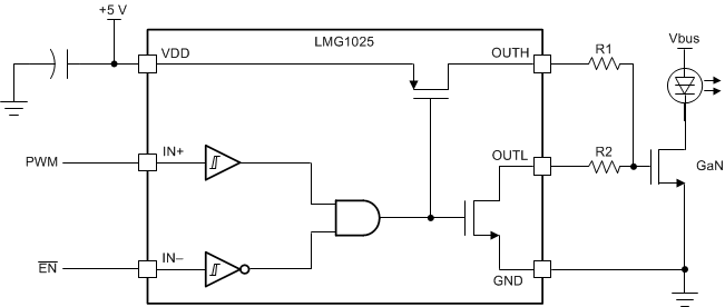
The LMG1025-Q1 is designed to be used with a single low-side, ground-referenced GaN or logic-level FET, as shown in Figure 6. Independent gate drive resistors, R1 and R2, are used to independently control the turnon and turnoff drive strengths, respectively. For fast and strong turnoff, R2 can be shorted and OUTL directly connected to the transistor’s gate. For symmetric drive strengths, it is acceptable to short OUTH and OUTL and use a single gate-drive resistor. The care should be taken that the ringing on the gate of the power device or ringing on any of the gate driver pin does not exceed the recommended rating. Resistors play an important role in damping these ringing. The layout and type of gate resistor with respect to gate driver and power device is also very important.
It is strongly recommended to use at least a 2-Ω resistor at each OUTH and OUTL to avoid voltage overstress due to inductive ringing. Ringing has to be ensured to be below VDD+0.3 V.
For applications requiring smaller resistance, please contact the factory for guidance.
 Figure 6. Typical Implementation of a Circuit