SNLS530D April 2016 – June 2018 LMH1219
PRODUCTION DATA.
- 1 Features
- 2 Applications
- 3 Description
- 4 Revision History
- 5 Pin Configuration and Functions
- 6 Specifications
-
7 Detailed Description
- 7.1 Overview
- 7.2 Functional Block Diagram
- 7.3
Feature Description
- 7.3.1 4-Level Input Configuration Pins
- 7.3.2 Input Carrier Detect
- 7.3.3 -6 dB Splitter Mode Launch Amplitude for IN0
- 7.3.4 Continuous Time Linear Equalizer (CTLE)
- 7.3.5 Input-Output Mux Selection
- 7.3.6 Clock and Data Recovery (CDR) Reclocker
- 7.3.7 Internal Eye Opening Monitor (EOM)
- 7.3.8 Output Function Control
- 7.3.9 Output Driver Amplitude and De-Emphasis Control
- 7.3.10 Status Indicators and Interrupts
- 7.3.11 Additional Programmability
- 7.4 Device Functional Modes
- 7.5 LMH1219 Register Map
- 8 Application and Implementation
- 9 Power Supply Recommendations
- 10Layout
- 11Device and Documentation Support
- 12Mechanical, Packaging, and Orderable Information
Package Options
Mechanical Data (Package|Pins)
- RTW|24
Thermal pad, mechanical data (Package|Pins)
- RTW|24
Orderable Information
8.2.4 Application Performance Plots
Depending on the selected input, the LMH1219 performance was measured with the test setups shown in Figure 23 and Figure 24.
 Figure 23. Test Setup for LMH1219 Cable Equalizer (IN0+)
 Figure 24. Test Setup for LMH1219 PCB Equalizer (IN1±)
The eye diagrams in this subsection show how the LMH1219 improves overall signal integrity in the data path for 75-Ω coax cable input length (CC) when IN0 is selected and 100-Ω differential FR4 PCB trace when IN1 is selected.
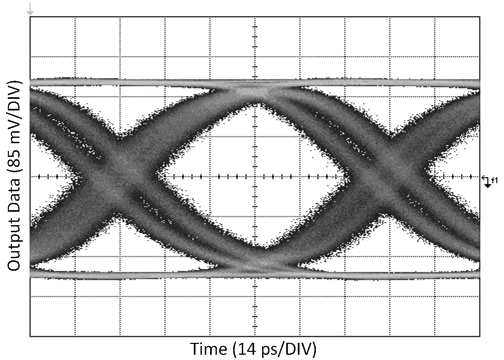
A. IN0 Selected, VOD_DE = H, IN_OUT_SEL = H, OUT_CTRL = L
Figure 25. 11.88 Gbps, CC = 75 m Belden 1694A,
EQ Only
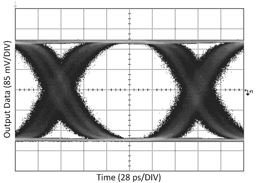
A. IN0 Selected, VOD_DE = H, IN_OUT_SEL = H, OUT_CTRL = L
Figure 27. 5.94 Gbps, CC = 120 m Belden 1694A,
EQ Only
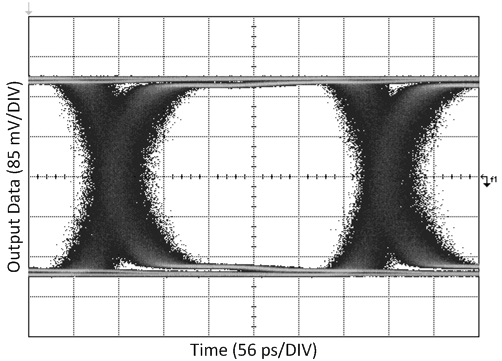
A. IN0 Selected, VOD_DE = H, IN_OUT_SEL = H, OUT_CTRL = L
Figure 29. 2.97 Gbps, CC = 200 m Belden 1694A,
EQ Only
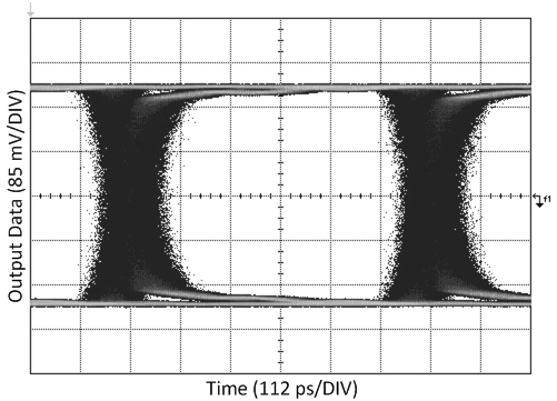
A. IN0 Selected, VOD_DE = H, IN_OUT_SEL = H, OUT_CTRL = L
Figure 31. 1.485 Gbps, CC = 280 m Belden 1694A,
EQ Only
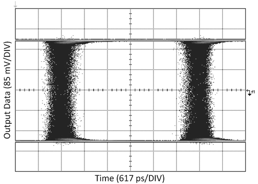
A. IN0 Selected, VOD_DE = H, IN_OUT_SEL = H, OUT_CTRL = L
Figure 33. 270 Mbps, CC = 600 m Belden 1694A,
EQ Only
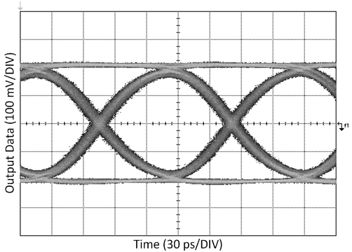
A. IN1 Selected, VOD_DE = H, IN_OUT_SEL = L, OUT_CTRL = L
Figure 35. 10.3125 Gbps, TL = 20 in. 5-Mil FR4,
EQ Only
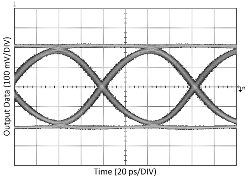
A. IN1 Selected, VOD_DE = H, IN_OUT_SEL = L, OUT_CTRL = L,
Override reference rate to lock to SMPTE rates
Figure 37. 11.88 Gbps, TL = 20 in. 5-Mil FR4,
Override reference rate to lock to SMPTE rates
EQ Only
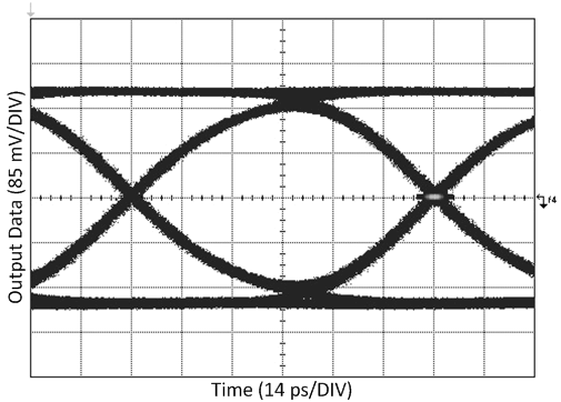
A. IN0 Selected, VOD_DE = H, IN_OUT_SEL = H, OUT_CTRL = F
Figure 26. 11.88 Gbps, CC = 75 m Belden 1694A,
Reclocked
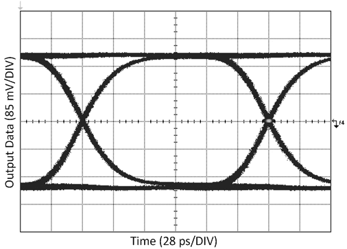
A. IN0 Selected, VOD_DE = H, IN_OUT_SEL = H, OUT_CTRL = F
Figure 28. 5.94 Gbps, CC = 120 m Belden 1694A,
Reclocked
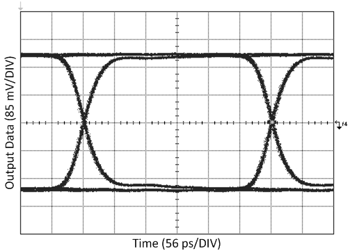
A. IN0 Selected, VOD_DE = H, IN_OUT_SEL = H, OUT_CTRL = F
Figure 30. 2.97 Gbps, CC = 200 m Belden 1694A,
Reclocked
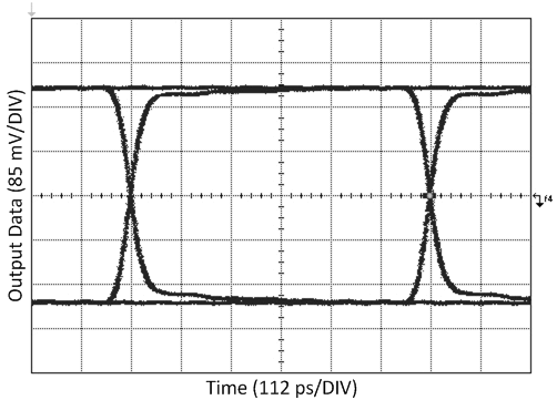
A. IN0 Selected, VOD_DE = H, IN_OUT_SEL = H, OUT_CTRL = F
Figure 32. 1.485 Gbps, CC = 280 m Belden 1694A,
Reclocked
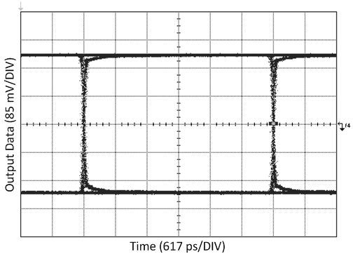
A. IN0 Selected, VOD_DE = H, IN_OUT_SEL = H, OUT_CTRL = F
Figure 34. 270 Mbps, CC = 600 m Belden 1694A,
Reclocked
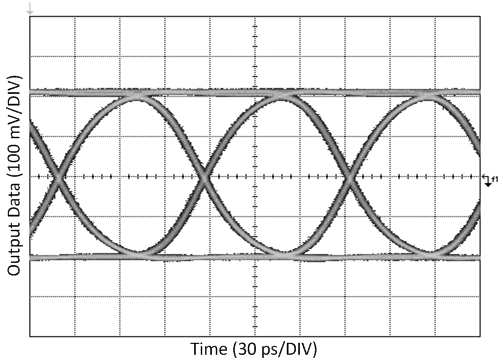
A. IN1 Selected, VOD_DE = H, IN_OUT_SEL = L, OUT_CTRL = F
Figure 36. 10.3125 Gbps, TL = 20 in. 5-Mil FR4,
Reclocked
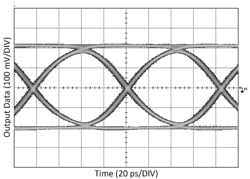
A. IN1 Selected, VOD_DE = H, IN_OUT_SEL = L, OUT_CTRL = F,
Override reference rate to lock to SMPTE rates
Figure 38. 11.88 Gbps, TL = 20 in. 5-Mil FR4,
Override reference rate to lock to SMPTE rates
Reclocked