SNLS530D April 2016 – June 2018 LMH1219
PRODUCTION DATA.
- 1 Features
- 2 Applications
- 3 Description
- 4 Revision History
- 5 Pin Configuration and Functions
- 6 Specifications
-
7 Detailed Description
- 7.1 Overview
- 7.2 Functional Block Diagram
- 7.3
Feature Description
- 7.3.1 4-Level Input Configuration Pins
- 7.3.2 Input Carrier Detect
- 7.3.3 -6 dB Splitter Mode Launch Amplitude for IN0
- 7.3.4 Continuous Time Linear Equalizer (CTLE)
- 7.3.5 Input-Output Mux Selection
- 7.3.6 Clock and Data Recovery (CDR) Reclocker
- 7.3.7 Internal Eye Opening Monitor (EOM)
- 7.3.8 Output Function Control
- 7.3.9 Output Driver Amplitude and De-Emphasis Control
- 7.3.10 Status Indicators and Interrupts
- 7.3.11 Additional Programmability
- 7.4 Device Functional Modes
- 7.5 LMH1219 Register Map
- 8 Application and Implementation
- 9 Power Supply Recommendations
- 10Layout
- 11Device and Documentation Support
- 12Mechanical, Packaging, and Orderable Information
Package Options
Mechanical Data (Package|Pins)
- RTW|24
Thermal pad, mechanical data (Package|Pins)
- RTW|24
Orderable Information
9 Power Supply Recommendations
The LMH1219 is designed to provide flexibility in supply rails. There are two ways to power the LMH1219:
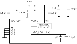
- Single Supply Mode (2.5 V): This mode offers ease of use, with the internal circuitry receiving power from the on-chip 1.8 V regulator. In this mode, 2.5 V is applied to VDD_CDR, VIN, and VDDIO. See Figure 39 for more details.
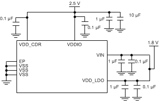
- Dual Supply Mode (2.5 V and 1.8 V): This mode provides lower power consumption. In this mode, 1.8 V is connected to both VIN and VDD_LDO. VDD_CDR, and VDDIO are powered from a 2.5 V supply. See Figure 40 for more details.
- When Dual Supply Mode is used, the 2.5 V supply for VDD_CDR and VDDIO should be powered before or at the same time as the 1.8 V supply that powers VIN and VDD_LDO.
 Figure 39. Typical Connection for Single 2.5 V Supply
 Figure 40. Typical Connection for Dual 2.5 V and 1.8 V Supply
For power supply de-coupling, 0.1-μF surface-mount ceramic capacitors are recommended to be placed close to each VDD_CDR, VIN, VDD_LDO, and VDDIO supply pin to VSS. Larger bulk capacitors (for example, 10 µF and 1 µF) are recommended for VDD_CDR and VIN. Good supply bypassing requires low inductance capacitors. This can be achieved through an array of multiple small body size surface-mount bypass capacitors in order to keep low supply impedance. Better results can be achieved through the use of a buried capacitor formed by a VDD and VSS plane separated by 2-4 mil dielectric in a printed circuit board.