SNLS530D April 2016 – June 2018 LMH1219
PRODUCTION DATA.
- 1 Features
- 2 Applications
- 3 Description
- 4 Revision History
- 5 Pin Configuration and Functions
- 6 Specifications
-
7 Detailed Description
- 7.1 Overview
- 7.2 Functional Block Diagram
- 7.3
Feature Description
- 7.3.1 4-Level Input Configuration Pins
- 7.3.2 Input Carrier Detect
- 7.3.3 -6 dB Splitter Mode Launch Amplitude for IN0
- 7.3.4 Continuous Time Linear Equalizer (CTLE)
- 7.3.5 Input-Output Mux Selection
- 7.3.6 Clock and Data Recovery (CDR) Reclocker
- 7.3.7 Internal Eye Opening Monitor (EOM)
- 7.3.8 Output Function Control
- 7.3.9 Output Driver Amplitude and De-Emphasis Control
- 7.3.10 Status Indicators and Interrupts
- 7.3.11 Additional Programmability
- 7.4 Device Functional Modes
- 7.5 LMH1219 Register Map
- 8 Application and Implementation
- 9 Power Supply Recommendations
- 10Layout
- 11Device and Documentation Support
- 12Mechanical, Packaging, and Orderable Information
Package Options
Mechanical Data (Package|Pins)
- RTW|24
Thermal pad, mechanical data (Package|Pins)
- RTW|24
Orderable Information
6.8 Typical Characteristics
TA = 25°C and VIN = VDDIO = VDD_CDR = 2.5 V (unless otherwise noted)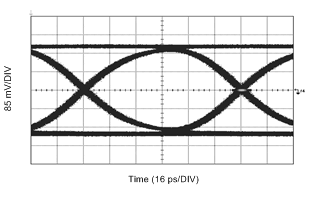 Figure 3. 10.3125 Gbps, IN1: 20 in. FR4 Trace
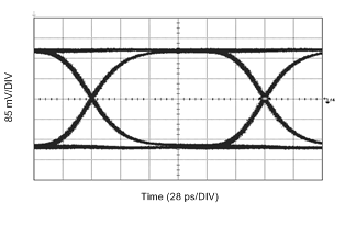 Figure 5. 5.94 Gbps, IN0: 120 m Belden 1694A
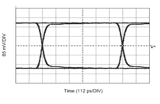 Figure 7. 1.485 Gbps, IN0: 280 m Belden 1694A
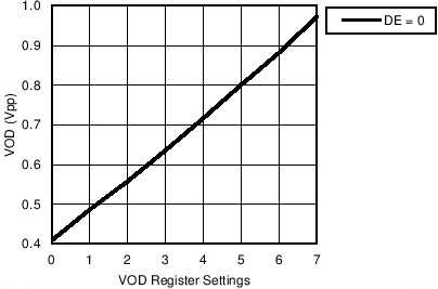 Figure 9. VOD vs. VOD and DEM Register Settings
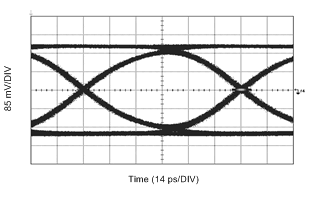 Figure 4. 11.88 Gbps, IN0: 75 m Belden 1694A
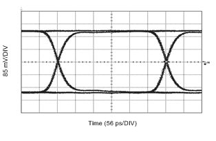 Figure 6. 2.97 Gbps, IN0: 200 m Belden 1694A
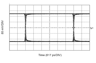 Figure 8. 270 Mbps, IN0: 600 m Belden 1694A
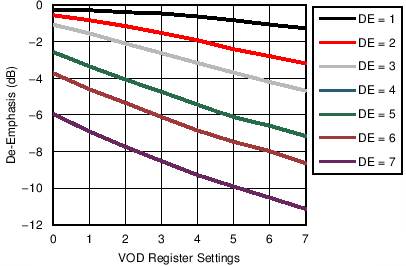 Figure 10. De-Emphasis vs. VOD and DEM Register Settings