SNAS636C December 2013 – July 2021 LMK00338
PRODUCTION DATA
- 1 Features
- 2 Applications
- 3 Description
- 4 Revision History
- 5 Pin Configuration and Functions
- 6 Specifications
- 7 Parameter Measurement Information
- 8 Detailed Description
- 9 Power Supply Recommendations
- 10Layout
- 11Device and Documentation Support
Package Options
Mechanical Data (Package|Pins)
- RTA|40
Thermal pad, mechanical data (Package|Pins)
- RTA|40
Orderable Information
5 Pin Configuration and Functions
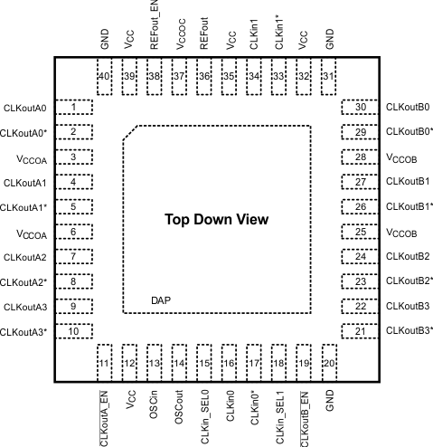
 Figure 5-1 RTA Package40-Pin WQFNTop View
Table 5-1 Pin Functions(3)
| PIN | TYPE | DESCRIPTION | |
|---|---|---|---|
| NAME | NO. | ||
| DAP | DAP | GND | Die Attach Pad. Connect to the PCB ground plane for heat dissipation. |
| CLKin0 | 16 | I | Universal clock input 0 (differential/single-ended) |
| CLKin0* | 17 | I | Universal clock input 0 (differential/single-ended) |
| CLKin1 | 34 | I | Universal clock input 1 (differential/single-ended) |
| CLKin1* | 33 | I | Universal clock input 1 (differential/single-ended) |
| CLKoutA_EN | 11 | I | Bank A low active output buffer enable(2) |
| CLKoutA0 | 1 | O | Differential clock output A0. |
| CLKoutA0* | 2 | O | Differential clock output A0. |
| CLKoutA1 | 4 | O | Differential clock output A1. |
| CLKoutA1* | 5 | O | Differential clock output A1. |
| CLKoutA2 | 7 | O | Differential clock output A2. |
| CLKoutA2* | 8 | O | Differential clock output A2. |
| CLKoutA3 | 9 | O | Differential clock output A3. |
| CLKoutA3* | 10 | O | Differential clock output A3. |
| CLKoutB_EN | 19 | I | Bank B low active output buffer enable(2) |
| CLKoutB1 | 27 | O | Differential clock output B1. |
| CLKoutB1* | 26 | O | Differential clock output B1. |
| CLKoutB0 | 30 | O | Differential clock output B0. |
| CLKoutB0* | 29 | O | Differential clock output B0. |
| CLKoutB2 | 24 | O | Differential clock output B2. |
| CLKoutB2* | 23 | O | Differential clock output B2. |
| CLKoutB3 | 22 | O | Differential clock output B3. |
| CLKoutB3* | 21 | O | Differential clock output B3. |
| CLKin_SEL0 | 15 | I | Clock input selection pins (2) |
| CLKin_SEL1 | 18 | I | Clock input selection pins (2) |
| GND | 20, 31, 40 | GND | Ground |
| OSCin | 13 | I | Input for crystal. Can also be driven by a XO, TCXO, or other external single-ended clock. |
| OSCout | 14 | O | Output for crystal. Leave OSCout floating if OSCin is driven by a single-ended clock. |
| REFout | 36 | O | LVCMOS reference output. Enable output by pulling REFout_EN pin high. |
| REFout_EN | 38 | I | REFout enable input. Enable signal is internally synchronized to selected clock input.(2) |
| VCC | 12, 32, 35, 39 | PWR | Power supply for Core and Input buffer blocks. The VCC supply operates from 3.3 V. Bypass with a 0.1-µF low-ESR capacitor placed very close to each VCC pin. |
| VCCOA | 3, 6 | PWR | Power supply for Bank A Output buffers. VCCOA can operate from 3.3 V or 2.5 V. The VCCOA pins are internally tied together. Bypass with a 0.1-µF low-ESR capacitor placed very close to each VCCO pin. (1) |
| VCCOB | 25, 28 | PWR | Power supply for Bank B Output buffers. VCCOB can operate from 3.3 V or 2.5 V. The VCCOB pins are internally tied together. Bypass with a 0.1-µF low-ESR capacitor placed very close to each VCCO pin. (1) |
| VCCOC | 37 | PWR | Power supply for REFout Output buffer. VCCOC can operate from 3.3 V or 2.5 V. Bypass with a 0.1-µF low-ESR capacitor placed very close to each VCCO pin.(1) |
(1) The output supply voltages/pins (VCCOA,
VCCOB, and VCCOC) is referred to generally as
VCCO when no distinction is needed, or when the output supply can
be inferred by the output bank/type.
(2) CMOS control input with internal pull-down resistor.
(3) Any unused output pins should be left floating with minimum
copper length (see note in Section 8.3.3), or properly terminated if connected to a transmission line, or
disabled/Hi-Z if possible. See Section 8.3.3 for output configuration or Section 9.2.2.1 output interface and termination techniques.