SNAS750B November   2020  – March 2021 LMK5C33216

PRODUCTION DATA  

  1. Features
  2. Applications
  3. Description
  4. Revision History
  5. Device Comparison
  6. Pin Configuration and Functions
  7. Specifications
    1. 7.1 Absolute Maximum Ratings
    2. 7.2 ESD Ratings
    3. 7.3 Recommended Operating Conditions
    4. 7.4 Thermal Information
    5. 7.5 Electrical Characteristics
    6. 7.6 Timing Diagrams
  8. Parameter Measurement Information
    1. 8.1 Differential Voltage Measurement Terminology
    2. 8.2 Output Clock Test Configurations
  9. Detailed Description
    1. 9.1 Overview
    2. 9.2 Functional Block Diagram
      1. 9.2.1 PLL Architecture Overview
      2. 9.2.2 DPLL
        1. 9.2.2.1 Independent DPLL Operation
        2. 9.2.2.2 Cascaded DPLL Operation
        3. 9.2.2.3 APLL Cascaded with DPLL
      3. 9.2.3 APLL-Only Mode
    3. 9.3 Feature Description
      1. 9.3.1  Oscillator Input (XO)
      2. 9.3.2  Reference Inputs
      3. 9.3.3  Clock Input Interfacing and Termination
      4. 9.3.4  Reference Input Mux Selection
        1. 9.3.4.1 Automatic Input Selection
        2. 9.3.4.2 Manual Input Selection
      5. 9.3.5  Hitless Switching
        1. 9.3.5.1 Hitless Switching with Phase Cancellation
        2. 9.3.5.2 Hitless Switching With Phase Slew Control
        3. 9.3.5.3 Hitless Switching With 1-PPS Inputs
      6. 9.3.6  Gapped Clock Support on Reference Inputs
      7. 9.3.7  Input Clock and PLL Monitoring, Status, and Interrupts
        1. 9.3.7.1 XO Input Monitoring
        2. 9.3.7.2 Reference Input Monitoring
          1. 9.3.7.2.1 Reference Validation Timer
          2. 9.3.7.2.2 Frequency Monitoring
          3. 9.3.7.2.3 Missing Pulse Monitor (Late Detect)
          4. 9.3.7.2.4 Runt Pulse Monitor (Early Detect)
          5. 9.3.7.2.5 Phase Valid Monitor for 1-PPS Inputs
        3. 9.3.7.3 PLL Lock Detectors
        4. 9.3.7.4 Tuning Word History
        5. 9.3.7.5 Status Outputs
        6. 9.3.7.6 Interrupt
      8. 9.3.8  PLL Relationships
        1. 9.3.8.1  PLL Frequency Relationships
          1. 9.3.8.1.1 APLL Phase Detector Frequency
          2. 9.3.8.1.2 APLL VCO Frequency
          3. 9.3.8.1.3 DPLL TDC Frequency
          4. 9.3.8.1.4 DPLL VCO Frequency
          5. 9.3.8.1.5 Clock Output Frequency
        2. 9.3.8.2  Analog PLLs (APLL1, APLL2, APLL3)
        3. 9.3.8.3  APLL Reference Paths
          1. 9.3.8.3.1 APLL XO Doubler
          2. 9.3.8.3.2 APLL XO Reference (R) Divider
        4. 9.3.8.4  APLL Phase Frequency Detector (PFD) and Charge Pump
        5. 9.3.8.5  APLL Feedback Divider Paths
          1. 9.3.8.5.1 APLL N Divider with SDM
        6. 9.3.8.6  APLL Loop Filters (LF1, LF2, LF3)
        7. 9.3.8.7  APLL Voltage Controlled Oscillators (VCO1, VCO2, VCO3)
          1. 9.3.8.7.1 VCO Calibration
        8. 9.3.8.8  APLL VCO Clock Distribution Paths
        9. 9.3.8.9  DPLL Reference (R) Divider Paths
        10. 9.3.8.10 DPLL Time-to-Digital Converter (TDC)
        11. 9.3.8.11 DPLL Loop Filter (DLF)
        12. 9.3.8.12 DPLL Feedback (FB) Divider Path
      9. 9.3.9  Output Clock Distribution
      10. 9.3.10 Output Channel Muxes
      11. 9.3.11 Output Dividers (OD)
      12. 9.3.12 SYSREF
      13. 9.3.13 Output Delay
      14. 9.3.14 Clock Outputs (OUTx_P/N)
        1. 9.3.14.1 Differential Output
        2. 9.3.14.2 LVCMOS Output
        3. 9.3.14.3 Output Auto-Mute During LOL
      15. 9.3.15 Glitchless Output Clock Start-Up
      16. 9.3.16 Clock Output Interfacing and Termination
      17. 9.3.17 Output Synchronization (SYNC)
      18. 9.3.18 Zero-Delay Mode (ZDM) Synchronization
      19. 9.3.19 Time of Day (ToD) Counter
        1. 9.3.19.1 Configuring ToD Functionality
        2. 9.3.19.2 SPI as a Trigger Source
        3. 9.3.19.3 GPIO Pin as a ToD Trigger Source
          1. 9.3.19.3.1 An Example: Making a time measurement using ToD and GPIO1 as trigger
        4. 9.3.19.4 ToD Timing
        5. 9.3.19.5 Other ToD Behavior
    4. 9.4 Device Functional Modes
      1. 9.4.1 Device Start-Up
        1. 9.4.1.1 ROM Selection
        2. 9.4.1.2 EEPROM Overlay
      2. 9.4.2 DPLL Operating States
        1. 9.4.2.1 Free-Run
        2. 9.4.2.2 Lock Acquisition
        3. 9.4.2.3 DPLL Locked
        4. 9.4.2.4 Holdover
      3. 9.4.3 PLL Start-Up Sequence
      4. 9.4.4 Digitally-Controlled Oscillator (DCO) Frequency and Phase Adjustment
        1. 9.4.4.1 DPLL DCO Control
          1. 9.4.4.1.1 DPLL DCO Relative Adjustment Frequency Step Size
          2. 9.4.4.1.2 APLL DCO Frequency Step Size
      5. 9.4.5 APLL Frequency Control
      6. 9.4.6 Zero-Delay Mode Synchronization
    5. 9.5 Programming
      1. 9.5.1 Interface and Control
      2. 9.5.2 I2C Serial Interface
        1. 9.5.2.1 I2C Block Register Transfers
      3. 9.5.3 SPI Serial Interface
        1. 9.5.3.1 SPI Block Register Transfer
      4. 9.5.4 Register Map Generation
      5. 9.5.5 General Register Programming Sequence
  10. 10Application and Implementation
    1. 10.1 Application Information
      1. 10.1.1 Device Start-Up Sequence
      2. 10.1.2 Power Down (PD#) Pin
      3. 10.1.3 Strap Pins for Start-Up
      4. 10.1.4 ROM and EEPROM
      5. 10.1.5 Power Rail Sequencing, Power Supply Ramp Rate, and Mixing Supply Domains
        1. 10.1.5.1 Power-On Reset (POR) Circuit
        2. 10.1.5.2 Powering Up From a Single-Supply Rail
        3. 10.1.5.3 Power Up From Split-Supply Rails
        4. 10.1.5.4 Non-Monotonic or Slow Power-Up Supply Ramp
      6. 10.1.6 Slow or Delayed XO Start-Up
    2. 10.2 Typical Application
      1. 10.2.1 Design Requirements
      2. 10.2.2 Detailed Design Procedure
    3. 10.3 Do's and Don'ts
  11. 11Power Supply Recommendations
    1. 11.1 Power Supply Bypassing
  12. 12Layout
    1. 12.1 Layout Guidelines
    2. 12.2 Layout Example
    3. 12.3 Thermal Reliability
      1. 12.3.1 Support for PCB Temperature up to 105°C
  13. 13Device and Documentation Support
    1. 13.1 Documentation Support
      1. 13.1.1 Related Documentation
    2. 13.2 Receiving Notification of Documentation Updates
    3. 13.3 Support Resources
    4. 13.4 Trademarks
    5. 13.5 Glossary
    6. 13.6 Electrostatic Discharge Caution
  14. 14Mechanical, Packaging, and Orderable Information

Package Options

Mechanical Data (Package|Pins)
Thermal pad, mechanical data (Package|Pins)
Orderable Information

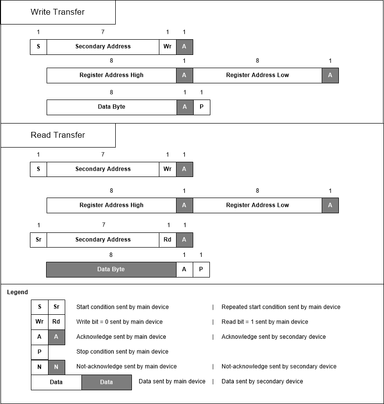
I2C Serial Interface

When (GPIO1 = 0), the device operates as an I2C client and supports bus rates of 100 kHz (standard mode) and 400 kHz (fast mode). Slower bus rates can work as long as the other I2C specifications are met. When operating with I2C communication interface the SCS_ADD pin selects one of three LSBs for the I2C device address. GPIO0 and GPIO2 input states determine device settings to load from ROM.

When using I2C communication the LMK5C33216 can support up to three different I2C addresses depending on the the state of the CSC_ADD pin on power-up, or any I2C address if the user re-programs the EEPROM. The five MSBs of the 7-bit I2C address are initialized from the EEPROM and the two LSBs are defined by the CSC_ADD pin state. The default EEPROM results in I2C addresses as shown in Table 9-7.

Table 9-7 I2C Address
CSC_ADD Pin State I2C Address LSB I2C Address
Low 0 0x64
Vmid 1 0x65
High 2 0x66
GUID-9D6FFA18-7D18-41CA-AC83-CCDC080373D1-low.gif Figure 9-41 I2C Byte Write and Read Transfers