SNVSB91C July   2019  – June 2020 LMR36506-Q1

PRODUCTION DATA.  

  1. Features
  2. Applications
  3. Description
    1.     Device Images
      1.      Simplified Schematic
      2.      Efficiency versus Output Current VOUT = 3.3 V (Fixed), 2.2 MHz
  4. Revision History
  5. Device Comparison Table
  6. Pin Configuration and Functions
    1.     Pin Functions
  7. Specifications
    1. 7.1 Absolute Maximum Ratings
    2. 7.2 ESD (Automotive) Ratings
    3. 7.3 Recommended Operating Conditions
    4. 7.4 Thermal Information
    5. 7.5 Electrical Characteristics
    6. 7.6 Timing Characteristics
    7. 7.7 Switching Characteristics
    8. 7.8 System Characteristics
    9. 7.9 Typical Characteristics
  8. Detailed Description
    1. 8.1 Overview
    2. 8.2 Functional Block Diagram
    3. 8.3 Feature Description
      1. 8.3.1  Enable, Start-up and Shutdown
      2. 8.3.2  External CLK SYNC (with MODE/SYNC)
        1. 8.3.2.1 Pulse-Dependent MODE/SYNC Pin Control
      3. 8.3.3  Adjustable Switching Frequency (with RT)
      4. 8.3.4  Power-Good Output Operation
      5. 8.3.5  Internal LDO, VCC UVLO, and VOUT/BIAS Input
      6. 8.3.6  Bootstrap Voltage and VCBOOT-UVLO (CBOOT Terminal)
      7. 8.3.7  Output Voltage Selection
      8. 8.3.8  Spread Spectrum
      9. 8.3.9  Soft Start and Recovery from Dropout
        1. 8.3.9.1 Recovery from Dropout
      10. 8.3.10 Current Limit and Short Circuit
      11. 8.3.11 Thermal Shutdown
      12. 8.3.12 Input Supply Current
    4. 8.4 Device Functional Modes
      1. 8.4.1 Shutdown Mode
      2. 8.4.2 Standby Mode
      3. 8.4.3 Active Mode
        1. 8.4.3.1 CCM Mode
        2. 8.4.3.2 Auto Mode - Light Load Operation
          1. 8.4.3.2.1 Diode Emulation
          2. 8.4.3.2.2 Frequency Reduction
        3. 8.4.3.3 FPWM Mode - Light Load Operation
        4. 8.4.3.4 Minimum On-time (High Input Voltage) Operation
        5. 8.4.3.5 Dropout
  9. Application and Implementation
    1. 9.1 Application Information
    2. 9.2 Typical Application
      1. 9.2.1 Design Requirements
      2. 9.2.2 Detailed Design Procedure
        1. 9.2.2.1 Choosing the Switching Frequency
        2. 9.2.2.2 Setting the Output Voltage
          1. 9.2.2.2.1 FB for Adjustable Output
        3. 9.2.2.3 Inductor Selection
        4. 9.2.2.4 Output Capacitor Selection
        5. 9.2.2.5 Input Capacitor Selection
        6. 9.2.2.6 CBOOT
        7. 9.2.2.7 VCC
        8. 9.2.2.8 CFF Selection
          1. 9.2.2.8.1 External UVLO
        9. 9.2.2.9 Maximum Ambient Temperature
      3. 9.2.3 Application Curves
    3. 9.3 What to Do and What Not to Do
  10. 10Power Supply Recommendations
  11. 11Layout
    1. 11.1 Layout Guidelines
      1. 11.1.1 Ground and Thermal Considerations
    2. 11.2 Layout Example
  12. 12Device and Documentation Support
    1. 12.1 Documentation Support
      1. 12.1.1 Related Documentation
    2. 12.2 Receiving Notification of Documentation Updates
    3. 12.3 Support Resources
    4. 12.4 Trademarks
    5. 12.5 Electrostatic Discharge Caution
    6. 12.6 Glossary
  13. 13Mechanical, Packaging, and Orderable Information

Package Options

Mechanical Data (Package|Pins)
Thermal pad, mechanical data (Package|Pins)
Orderable Information

Dropout

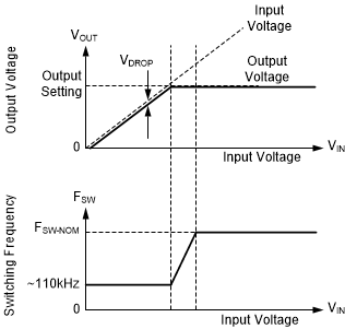
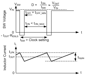
Dropout operation is defined as any input-to-output voltage ratio that requires frequency to drop to achieve the required duty cycle. At a given clock frequency, duty cycle is limited by minimum off-time. Once this limit is reached as shown in Figure 29 if clock frequency was to be maintained, the output voltage would fall. Instead of allowing the output voltage to drop, the LMR36506-Q1 extends the high side switch on-time past the end of the clock cycle until the needed peak inductor current is achieved. The clock is allowed to start a new cycle once peak inductor current is achieved or once a pre-determined maximum on-time, tON-MAX, of approximately 9 µs passes. As a result, once the needed duty cycle cannot be achieved at the selected clock frequency due to the existence of a minimum off-time, frequency drops to maintain regulation. As shown in Figure 28 if input voltage is low enough so that output voltage cannot be regulated even with an on-time of tON-MAX, output voltage drops to slightly below the input voltage by VDROP. For additional information on recovery from dropout, refer back to Figure 17.
LMR36506-Q1 MODEdropChart.gif
Output voltage and frequency versus input voltage: If there is little difference between input voltage and output voltage setting, the IC reduces frequency to maintain regulation. If input voltage is too low to provide the desired output voltage at approximately 110 kHz, input voltage tracks output voltage.
Figure 28. Frequency and Output Voltage in Dropout
LMR36506-Q1 MODEdropWFM.gif
Switching waveforms while in dropout. Inductor current takes longer than a normal clock to reach the desired peak value. As a result, frequency drops. This frequency drop is limited by tON-MAX.
Figure 29. Dropout Waveforms