SNVSB91C July 2019 – June 2020 LMR36506-Q1
PRODUCTION DATA.
- 1 Features
- 2 Applications
- 3 Description
- 4 Revision History
- 5 Device Comparison Table
- 6 Pin Configuration and Functions
- 7 Specifications
-
8 Detailed Description
- 8.1 Overview
- 8.2 Functional Block Diagram
- 8.3
Feature Description
- 8.3.1 Enable, Start-up and Shutdown
- 8.3.2 External CLK SYNC (with MODE/SYNC)
- 8.3.3 Adjustable Switching Frequency (with RT)
- 8.3.4 Power-Good Output Operation
- 8.3.5 Internal LDO, VCC UVLO, and VOUT/BIAS Input
- 8.3.6 Bootstrap Voltage and VCBOOT-UVLO (CBOOT Terminal)
- 8.3.7 Output Voltage Selection
- 8.3.8 Spread Spectrum
- 8.3.9 Soft Start and Recovery from Dropout
- 8.3.10 Current Limit and Short Circuit
- 8.3.11 Thermal Shutdown
- 8.3.12 Input Supply Current
- 8.4 Device Functional Modes
-
9 Application and Implementation
- 9.1 Application Information
- 9.2
Typical Application
- 9.2.1 Design Requirements
- 9.2.2 Detailed Design Procedure
- 9.2.3 Application Curves
- 9.3 What to Do and What Not to Do
- 10Power Supply Recommendations
- 11Layout
- 12Device and Documentation Support
- 13Mechanical, Packaging, and Orderable Information
Package Options
Mechanical Data (Package|Pins)
- RPE|9
Thermal pad, mechanical data (Package|Pins)
- RPE|9
Orderable Information
8.3.9.1 Recovery from Dropout
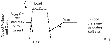
Any time the output voltage falls more than a few percent, output voltage ramps up slowly. This condition, called graceful recovery from dropout in this document, differs from soft start in two important ways:
- The reference voltage is set to approximately 1% above what is needed to achieve the existing output voltage.
- If the device is set to FPWM, it will continue to operate in that mode during its recovery from dropout. If output voltage were to suddenly be pulled up by an external supply, the LMR36506-Q1 can pull down on the output. Note that all protections that are present during normal operation are in place, preventing any catastrophic failure if output is shorted to a high voltage or ground.
 Figure 17. Recovery from Dropout
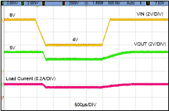
  Figure 18. Typical Output Recovery from Dropout from 8 V to 4 V
 Whether output voltage falls due to high load or low input voltage, once the condition that causes output to fall below its set point is removed, the output climbs at the same speed as during start-up. shows an example of this behavior.