SLCS136V August 1999 – May 2025 LMV331 , LMV339 , LMV393
PRODUCTION DATA
- 1
- 1 Features
- 2 Applications
- 3 Description
- 4 Pin Configuration and Functions
-
5 Specifications
- 5.1 Absolute Maximum Ratings
- 5.2 ESD Ratings
- 5.3 Recommended Operating Conditions
- 5.4 Thermal Information
- 5.5 Electrical Characteristics, VCC+ = 2.7V
- 5.6 Switching Characteristics, VCC+ = 2.7V
- 5.7 Electrical Characteristics, VCC+ = 5V
- 5.8 Switching Characteristics, VCC+ = 5V
- 5.9 Typical Characteristics
- 6 Detailed Description
- 7 Application and Implementation
- 8 Power Supply Recommendations
- 9 Layout
- 10Device and Documentation Support
- 11Trademarks
- 12Electrostatic Discharge Caution
- 13Glossary
- 14Revision History
- 15Mechanical, Packaging, and Orderable Information
Package Options
Refer to the PDF data sheet for device specific package drawings
Mechanical Data (Package|Pins)
- DBV|5
- DCK|5
Thermal pad, mechanical data (Package|Pins)
Orderable Information
4 Pin Configuration and Functions
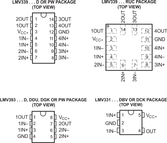
Table 4-1 Pin Functions
| PIN | TYPE | DESCRIPTION | ||||
|---|---|---|---|---|---|---|
| NAME | LMV331 | LMV393 | LMV339 | |||
| DBV, DCK | D, DGK , PW | D, PW | RUC | |||
| 1IN– , 2IN–, 3IN–, 4IN– | 3 | 2, 6 | 4, 6, 8, 10 | 3, 5, 7, 9 | I | Comparator negative input pin |
| 1IN+ , 2IN+, 3IN+, 4IN+ | 1 | 3, 5 | 5, 7, 9, 11 | 4, 6, 8, 10 | I | Comparator positive input pin |
| GND | 2 | 4 | 12 | 11 | I | Ground |
| 1OUT, 2OUT, 3OUT, 4OUT | 4 | 1, 7 | 2, 1, 14, 13 | 1, 14, 13, 12 | O | Comparator output pin |
| VCC+ | 5 | 8 | 3 | 2 | I | Supply Pin |