SGLS342D July 2006 – July 2025 LMV341-Q1 , LMV344-Q1
PRODUCTION DATA
- 1
- 1Features
- 2Description
- 3Device Comparison Table
- 4Pin Configuration and Functions
- 5Specifications
- 6Typical Characteristics
- 7Device and Documentation Support
- 8Revision History
- 9Mechanical, Packaging, and Orderable Information
Package Options
Mechanical Data (Package|Pins)
Thermal pad, mechanical data (Package|Pins)
Orderable Information
6 Typical Characteristics
 Figure 6-1 Supply Current
vs
Supply Voltage
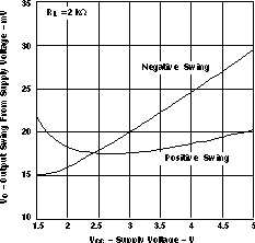 Figure 6-3 Output Voltage Swing
vs
Supply Voltage
 Figure 6-5 Source Current
vs
Output Voltage
 Figure 6-7 Sink Current
vs
Output Voltage
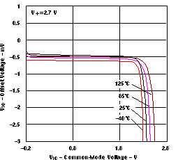 Figure 6-9 Offset Voltage
vs
Common-mode Voltage
 Figure 6-11 Input Voltage
vs
Output Voltage
 Figure 6-13 Slew Rate
vs
Supply Voltage
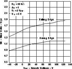 Figure 6-15 Slew Rate
vs
Temperature
 Figure 6-17 Psrr
vs
Frequency
 Figure 6-19 Total Harmonic Distortion + Noise
vs
Frequency
 Figure 6-2 Input Bias Current
vs
Temperature
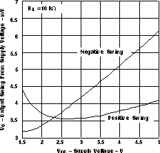 Figure 6-4 Output Voltage Swing
vs
Supply Voltage
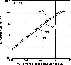 Figure 6-6 Source Current
vs
Output Voltage
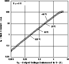 Figure 6-8 Sink Current
vs
Output Voltage
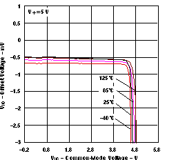 Figure 6-10 Offset Voltage
vs
Common-mode Voltage
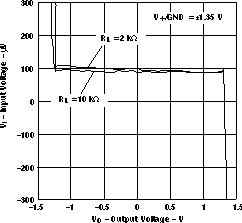 Figure 6-12 Input Voltage
vs
Output Voltage
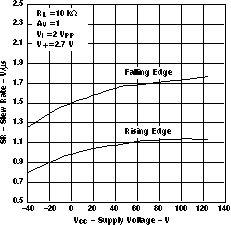 Figure 6-14 Slew Rate
vs
Temperature
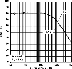 Figure 6-16 Cmrr
vs
Frequency
 Figure 6-18 Input Voltage Noise
vs
Frequency
 Figure 6-20 Total Harmonic Distortion + Noise
vs
Output Voltage
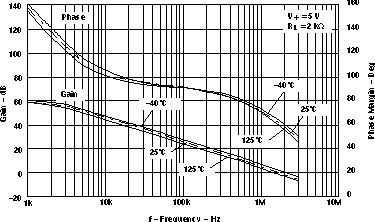 Figure 6-21 Gain And Phase Margin
vs
Frequency
(ta = –40°c, 25°c, 125°c)
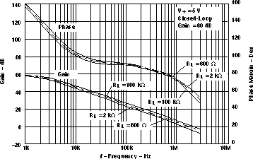 Figure 6-23 Gain And Phase Margin
vs
Frequency
(rl = 600ω, 2kω, 100kω)
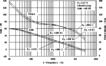 Figure 6-22 Gain And Phase Margin
vs
Frequency
(rl = 600ω, 2kω, 100kω)
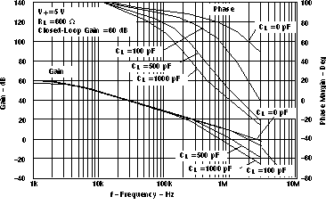 Figure 6-24 Gain And Phase Margin
vs
Frequency
(cl = 0pf, 100pf, 500pf, 1000pf)
 Figure 6-25 Small-Signal Noninverting Response
 Figure 6-27 Small-Signal Noninverting Response
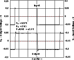 Figure 6-29 Small-Signal Noninverting Response
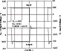 Figure 6-31 Small-Signal Inverting Response
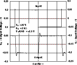 Figure 6-33 Small-Signal Inverting Response
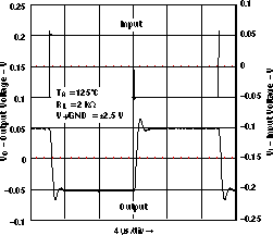 Figure 6-35 Small-Signal Inverting Response
 Figure 6-26 Large-Signal Noninverting Response
 Figure 6-28 Large-Signal Noninverting Response
 Figure 6-30 Large-Signal Noninverting Response
 Figure 6-32 Large-Signal Inverting Response
 Figure 6-34 Large-Signal Inverting Response
 Figure 6-36 Large-Signal Inverting Response