SGLS342D July 2006 – July 2025 LMV341-Q1 , LMV344-Q1
PRODUCTION DATA
- 1
- 1Features
- 2Description
- 3Device Comparison Table
- 4Pin Configuration and Functions
- 5Specifications
- 6Typical Characteristics
- 7Device and Documentation Support
- 8Revision History
- 9Mechanical, Packaging, and Orderable Information
Package Options
Mechanical Data (Package|Pins)
Thermal pad, mechanical data (Package|Pins)
Orderable Information
2 Description
The LMV341 and LMV344 devices are single and quad CMOS operational amplifiers, respectively, with low voltage, low power, and rail-to-rail output swing capabilities. The PMOS input stage offers an ultra-low input bias current of 1pA (typical) and an offset voltage of 0.25mV (typical). The single supply amplifier is designed specifically for low-voltage (2.7V to 5V) operation, with a wide common-mode input voltage range that typically extends from –0.2Vto 0.8V from the positive supply rail. Additional features are a 20nV/√ Hz voltage noise at 10kHz, 1MHz unity-gain bandwidth, 1V/μs slew rate, and 100μA current consumption per channel.
An extended industrial temperature range from –40°C to 125°C makes this device an excellent choice for automotive applications.
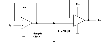
 Application Circuit: Sample-and-Hold Circuit