SNAS783C June   2020  – February 2021 LMX2820

PRODUCTION DATA  

  1. Features
  2. Applications
  3. Description
  4. Revision History
  5. Pin Configuration and Functions
  6. Specifications
    1. 6.1 Absolute Maximum Ratings
    2. 6.2 ESD Ratings
    3. 6.3 Recommended Operating Conditions
    4. 6.4 Thermal Information
    5. 6.5 Electrical Characteristics
    6. 6.6 Timing Requirements
    7. 6.7 Typical Characteristics
  7. Detailed Description
    1. 7.1 Overview
    2. 7.2 Functional Block Diagram
    3. 7.3 Feature Description
      1. 7.3.1  Reference Oscillator Input
      2. 7.3.2  Input Path
        1. 7.3.2.1 Input Path Doubler (OSC_2X)
        2. 7.3.2.2 Pre-R Divider (PLL_R_PRE)
        3. 7.3.2.3 Programmable Input Multiplier (MULT)
        4. 7.3.2.4 R Divider (PLL_R)
      3. 7.3.3  PLL Phase Detector and Charge Pump
      4. 7.3.4  N Divider and Fractional Circuitry
        1. 7.3.4.1 Integer N Divide Portion (PLL_N)
        2. 7.3.4.2 Fractional N Divide Portion (PLL_NUM and PLL_DEN)
        3. 7.3.4.3 Modulator Order (MASH_ORDER)
      5. 7.3.5  LD Pin Lock Detect
      6. 7.3.6  MUXOUT Pin and Readback
      7. 7.3.7  Internal VCO
        1. 7.3.7.1 VCO Calibration
          1. 7.3.7.1.1 Determining the VCO Gain and Ranges
      8. 7.3.8  Channel Divider
      9. 7.3.9  Output Frequency Doubler
      10. 7.3.10 Output Buffer
      11. 7.3.11 Power-Down Modes
      12. 7.3.12 Phase Synchronization for Multiple Devices
        1. 7.3.12.1 SYNC Categories
        2. 7.3.12.2 Phase Adjust
          1. 7.3.12.2.1 Using MASH_SEED to Create a Phase Shift
          2. 7.3.12.2.2 Static vs. Dynamic Phase Adjust
          3. 7.3.12.2.3 Fine Adjustments to Phase Adjust
      13. 7.3.13 SYSREF
      14. 7.3.14 Fast VCO Calibration
      15. 7.3.15 Double Buffering (Shadow Registers)
      16. 7.3.16 Output Mute Pin and Ping Pong Approaches
    4. 7.4 Device Functional Modes
      1. 7.4.1 External VCO Mode
      2. 7.4.2 External Feedback Input Pins
        1. 7.4.2.1 PFDIN External Feedback Mode
        2. 7.4.2.2 RFIN External Feedback Mode
  8. Application and Implementation
    1. 8.1 Application Information
      1. 8.1.1 Treatment of Unused Pins
      2. 8.1.2 External Loop Filter
      3. 8.1.3 Using Instant Calibration
    2. 8.2 Typical Application
      1. 8.2.1 Design Requirements
      2. 8.2.2 Detailed Design Procedure
      3. 8.2.3 Application Curves
    3. 8.3 Initialization and Power-on Sequencing
  9. Power Supply Recommendations
  10. 10Layout
    1. 10.1 Layout Guidelines
    2. 10.2 Layout Example
  11. 11Device and Documentation Support
    1. 11.1 Receiving Notification of Documentation Updates
    2. 11.2 Support Resources
    3. 11.3 Trademarks
    4. 11.4 Electrostatic Discharge Caution
    5. 11.5 Glossary
  12. 12Mechanical, Packaging, and Orderable Information

Package Options

Mechanical Data (Package|Pins)
Thermal pad, mechanical data (Package|Pins)
Orderable Information

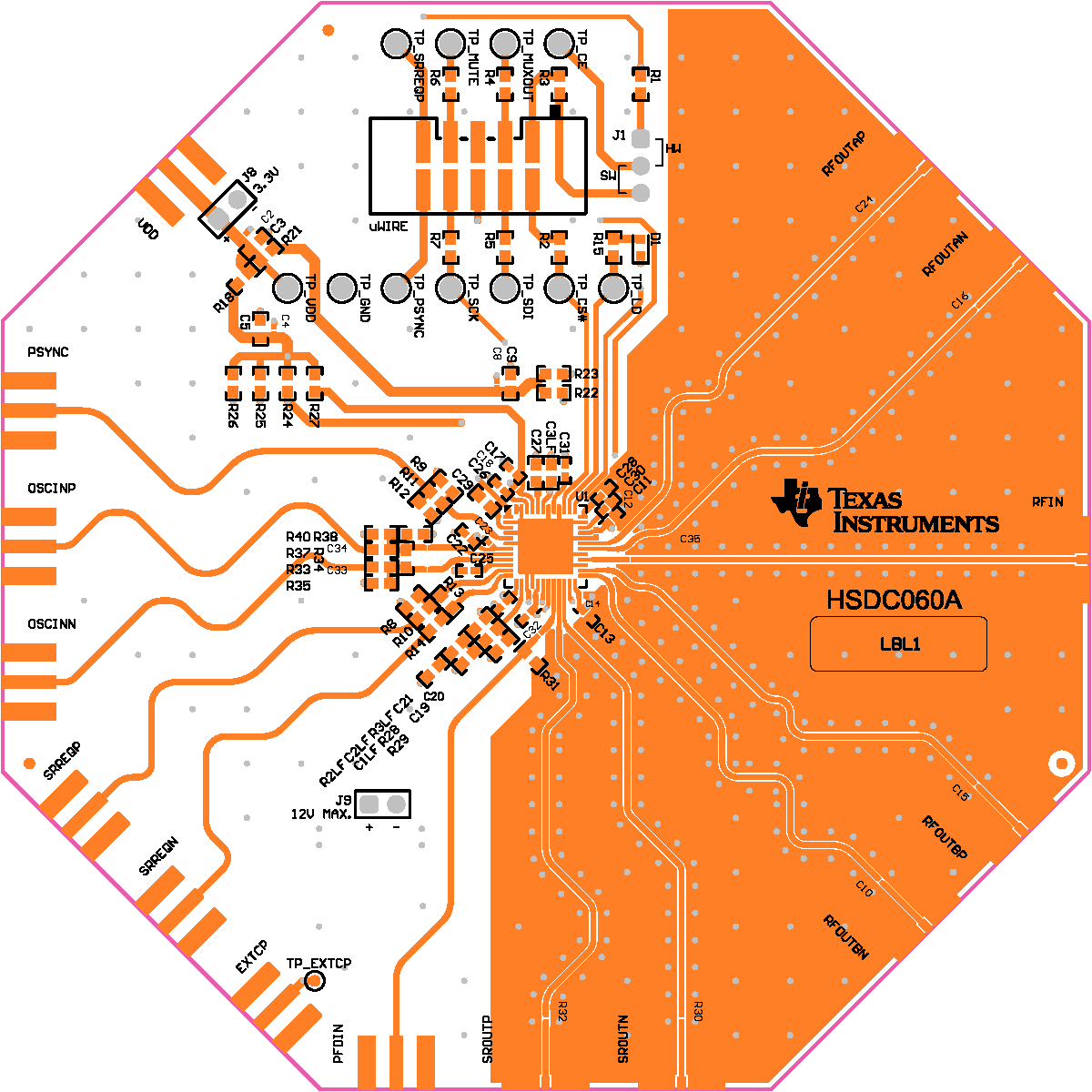
Layout Example

For this layout, all of the loop filter (C1LF, C2LF, C3LF, R2LF and R3LF) are on the top side of the board. C3LF is located right next to the VTUNE pin. In the event that this C3LF capacitor would be open, TI recommends to move one of loop capacitors in this spot. For instance, if a second order loop filter was used, technically C3LF would be open. However, for this layout example that is designed for a third order loop filter, it would be optimal to make C1LF = open, and C3LF to be whatever C1LF would have been.
GUID-A3C5330E-8AFA-4E1D-BCCA-B10426F11CEF-low.pngFigure 10-1 Layout Example