SNVS345G June 2006 – December 2014 LP5951
PRODUCTION DATA.
- 1 Features
- 2 Applications
- 3 Description
- 4 Revision History
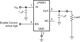
- 5 Pin Configuration and Functions
- 6 Specifications
- 7 Detailed Description
- 8 Application and Implementation
- 9 Power Supply Recommendations
- 10Layout
- 11Device and Documentation Support
- 12Mechanical, Packaging, and Orderable Information
Package Options
Mechanical Data (Package|Pins)
Thermal pad, mechanical data (Package|Pins)
Orderable Information
1 Features
- Input Voltage Range: 1.8 V to 5.5 V
- Output Voltage Range: 1.3 V to 3.7 V
- Excellent Line Transient Response: ±2 mV (typical)
- Excellent PSRR: –60 dB at 1 kHz typical
- Low Quiescent Current of 29 µA typical
- Small SC70-5 and SOT-23-5 Packages
- Fast Turnon Time of 30 µs typ.
- Typical < 1 nA Quiescent Current in Shutdown
- Ensured 150-mA Output Current
- Logic Controlled Enable 0.4 V/0.9 V
- Good Load Transient Response of 50 mVpp (typical)
- Thermal Overload and Short-Circuit Protection
- -40°C to 125°C Junction Temperature Range
2 Applications
General Purpose
3 Description
The LP5951 regulator is designed to meet the requirements of portable battery-powered systems providing a regulated output voltage and low quiescent current. When switched to shutdown mode via a logic signal at the Enable (EN) pin, the power consumption is reduced to virtually zero.
The LP5951 is designed to be stable with small 1-µF ceramic capacitors. The device also features internal protection against short-circuit currents and over-temperature conditions.
Performance is specified for a –40°C to 125°C temperature range.
The device is available in fixed output voltages in the range of 1.3 V to 3.7 V. For availability, please contact your local TI sales office.
Device Information(1)
| PART NUMBER | PACKAGE | BODY SIZE (NOM) |
|---|---|---|
| LP5951 | SOT-23 (5) | 2.90 mm x 1.60 mm |
| SC70 (5) | 2.00 mm x 1.25 mm |
- For all available packages, see the orderable addendum at the end of the datasheet.
Simplified Schematic