SNVS345G June 2006 – December 2014 LP5951
PRODUCTION DATA.
- 1 Features
- 2 Applications
- 3 Description
- 4 Revision History
- 5 Pin Configuration and Functions
- 6 Specifications
- 7 Detailed Description
- 8 Application and Implementation
- 9 Power Supply Recommendations
- 10Layout
- 11Device and Documentation Support
- 12Mechanical, Packaging, and Orderable Information
Package Options
Mechanical Data (Package|Pins)
Thermal pad, mechanical data (Package|Pins)
Orderable Information
10 Layout
10.1 Layout Guidelines
The dynamic performance of the LP5951 is dependent on the layout of the PCB. PCB layout practices that are adequate for typical LDOs may degrade the load regulation, PSRR, noise, or transient performance of the LP5951. Best performance is achieved by placing CIN and COUT on the same side of the PCB as the LP5951, and as close as is practical to the package. The ground connections for CIN and COUT should be back to the LP5951 ground pin using as wide, and as short, of a copper trace as is practical.
Connections using long trace lengths, narrow trace widths, and/or connections through vias should be avoided. These will add parasitic inductances and resistance that results in inferior performance especially during transient conditions.
A Ground Plane, either on the opposite side of a two-layer PCB, or embedded in a multi-layer PCB, is strongly recommended. This Ground Plane serves as a circuit reference plane to assure accuracy.
10.2 Layout Example
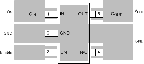 Figure 15. LP5951 Layout